semi合集-English.pdf - 第5190页
SEMI M34-0299 © SEMI 1999 8 Table 2. Example SIMOX Wafer Surface Inspectio n Criteria Criterion Allow Quantity Description Slip 0.3 mm: NONE 0.1 − 0.3 mm: < 15 mm total < 0.1 mm: OVERLOOK 6 mm edge exclusion Scratc…
SEMI M34-0299 © SEMI 1999 7
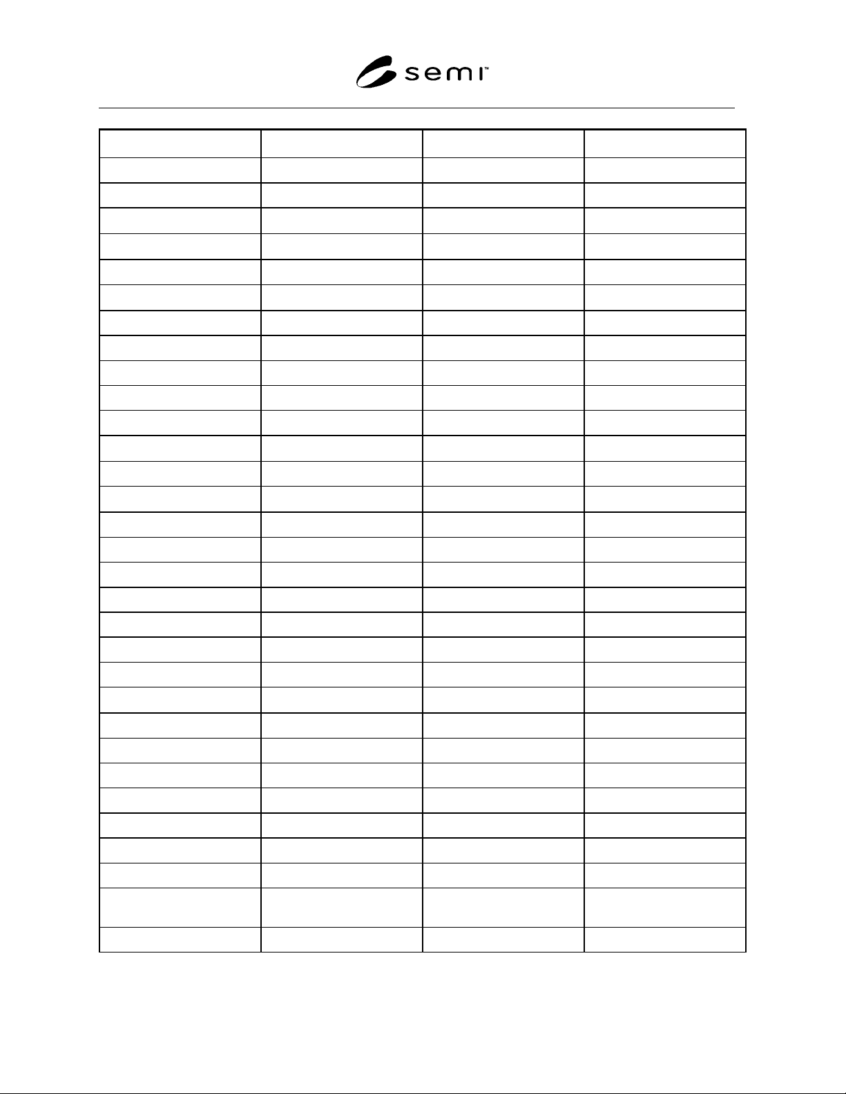
Table 1. Specification Summary
Parameter Reference Example Values Method
Wafer diameter (D) ASTM 613 150 mm, 200 mm Optical comparitor
Wafer thickness ASTM 533 Thickness gauge
Thickness variation ASTM 533
< 3 µm
Thickness gauge
Wafer warp ASTM F 657, F 1390
≤ 30 µm for D = 150 mm
Jig + gauge
Crystal orientation ASTM 26 X-ray diffraction
a) front surface
(100) ± 1°
b) back surface
Substrate type/dopant ASTM 42 Hot point probe
Substrate resistivity ASTM 84 4-point probe
Substrate RRG ASTM 84 4-point probe
Surface Si thickness Section 7.1.5 50 nm to 500 nm SE/optical reflectance
Surface Si uniformity Section 7.1.3
± 5 nm
SE/optical reflectance
Buried oxide thickness Section 7.1.6 50 nm to 500 nm SE/optical reflectance
Buried OX uniformity Section 7.1.3
± 10 nm
SE/optical reflectance
Crystal defect (EPD) Section 7.2 < 10 E7/cm
2
SEM examination
Secco etch
Buried OX pinholes < 0.1/cm
2
a) CuSO
4
plating
b) BOX capacitor @ 1 nA
Metal contamination Section 7.4.1 total < 10
11
atoms /cm
2
TXRF
a) per unit area
b) per unit volume
Particles Section 7.4.2
≤ 20 (> 0.25 µm) / wafer
Automated particle counter
Haze Section 7.4.3 See Table 2. Visual inspection
Slip ASTM F 523* See Table 2. Visual inspection
Scratches ASTM F 523* None Visual inspection
Chips ASTM F 523* See Table 2. Visual inspection
Surf Spot Discolor ASTM F 523 See Table 2. Visual inspection
Foreign matter ASTM F 523 See Table 2. Visual inspection
Backside contamination ASTM F 523 Visual inspection
Surface roughness Section 7.4.4 5 Atomic force microscope
(AFM)
Inclusions Section 7.4.5
* The user and supplier may agree on an edge exclusion for these specifications. For example, the area within 6 mm proximity of
the wafer edge may be excluded.
SEMI M34-0299 © SEMI 1999 8
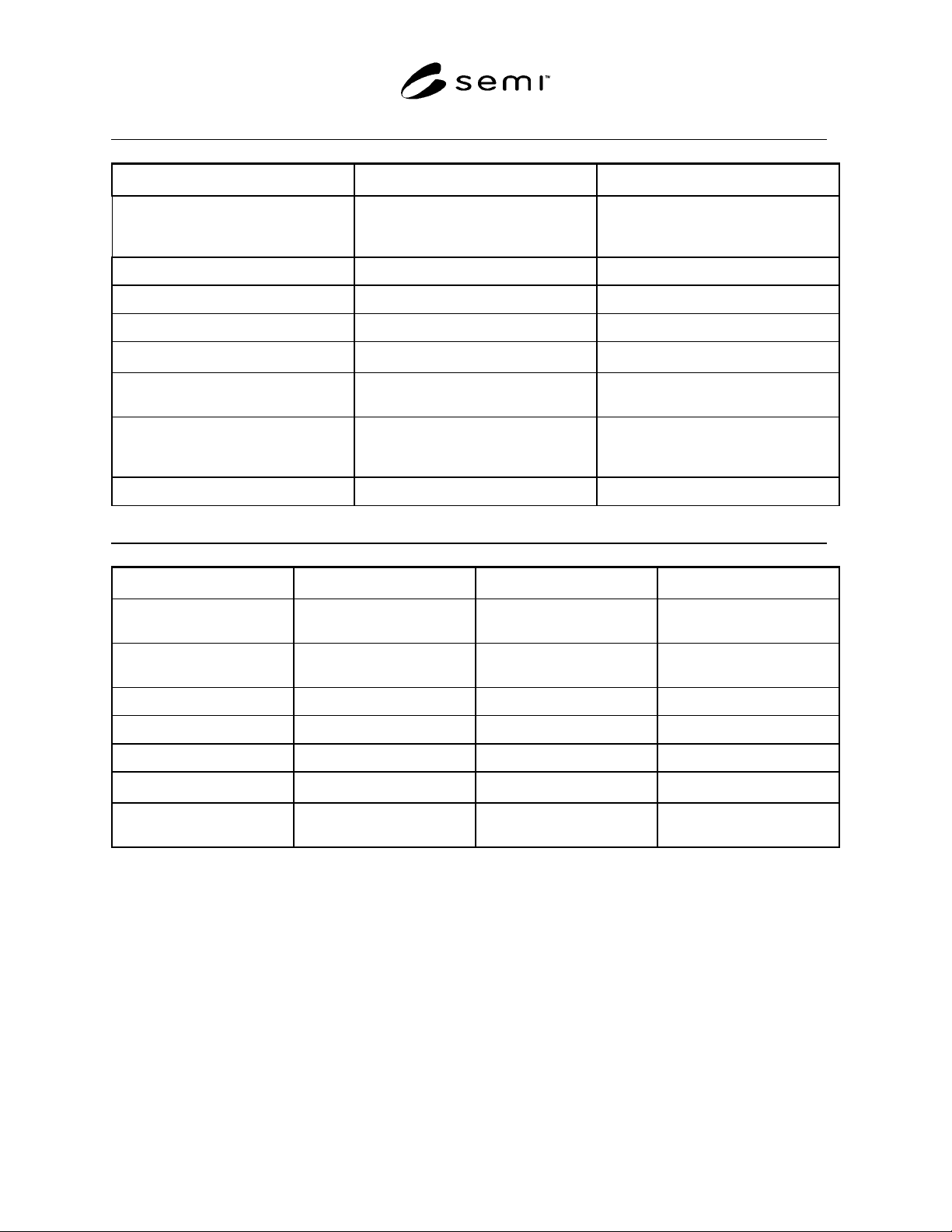
Table 2. Example SIMOX Wafer Surface Inspection Criteria
Criterion Allow Quantity Description
Slip 0.3 mm: NONE
0.1−0.3 mm: < 15 mm total
< 0.1 mm: OVERLOOK
6 mm edge exclusion
Scratch NONE 6 mm edge exclusion
Contamination NONE Backside
Stain < 5 spots < 0.05 cm
2
total area
Edge Chips/Cracks < 1.5 mm circumferential < 1.8 mm radial
combined length 1 × bright light
Pits and Dimples < 0.5 mm - 10/wafer
> 0.5 mm - NONE
1 × bright light
Haze Moderate haze - NONE
Heavy haze - NONE
Non-uniform haze - NONE
Light uniform haze is acceptable.
(Iterate between user and vendor.)
Foreign Matter (embedded particles) < 0.05/cm
2
< 3 embedded particles per 150 mm wafer
Table 3. SIMOX Electrical Parameters
Parameters Reference Value Method
Photoconductivity Lifetime
(Backside)
Section 8.1
> 1 msec.
microwave
Photoconductivity Lifetime
(Front side)
Section 8.1 TBD microwave
BOX Breakdown Section 8.2 > 5 MV/cm I-V
BOX Pinholes Section 8.3 < 0.2 cm
2
I-V
BOX Charge Section 8.4 < C-V
BOX Surface States Section 8.5
< 5 × 10
10
/cm
2
C-V
Doping Density
Sub, Surface
Section 8.6 TBD 4-point probe
8. Electrical Parameters
8.1 Photoconductivity Lifetime — This is measured by
creating an excess of carriers (typically by using a light
source) and measuring the slope of the decay curve.
Several pieces of commercial equipment are available
for this purpose. This requires that polysilicon is not
deposited on the backside, as is sometimes done for
gettering. Also, surface passivation may be needed for
lifetime measurements. Backside measurements
indicate the quality of the substrate and can be
performed by traditional methods. Frontside
measurements are more difficult and must be performed
using incident light which can be entirely absorbed
before reaching the underlying substrate.
8.1.1 Typically, the sample is placed on a micro-wave
wave guide post, forming part of a transmission line
circuit. The microwave reflection is determined by the
total conductivity of the sample and the conductivity is
modulated by an intense light pulse. When the light is
turned off, the microwave detects an exponential decay
in conductivity from which a decay constant is
determined. The photoconductivity lifetime is a result
of the recombination velocity at the surfaces, volume
recombination in the silicon layer, and any trapping.
Measurements are made independently on the front and

SEMI M34-0299 © SEMI 1999 9
back sides of the wafer. The mean value on the
backside of the wafer will typically be at least 10
microseconds for N-type material and 3 microseconds
for P-type material. These values correspond to about a
100 micron diffusion length (SPV value).
8.1.2 The relevance of photoconductivity lifetime to
the users requirement should be discussed. The use of
this measurement should be negotiated between
customer and vendor.
8.2 BOX Breakdown This parameter can be
measured with a buried oxide capacitor (BOX-CAP).
The buried oxide thickness and the intended application
will affect both the test procedure (such as capacitor
area and voltage criterion) and the allowable values of
measured parameters. These should be determined by
agreement between the user and vendor. Example
procedure and values for standard evaluation of 400 nm
thick buried oxide are given in the following
paragraphs.
8.2.1 Test Structure — Buried oxide capacitor (BOX-
CAP) having an area of 0.01 cm
2
for standard (400 nm)
BOX. The electrode material and thickness affect the
breakdown phenomena due to thermal effects, and so
should be included in the agreement between customer
and vendor.
8.2.2 Test Method: Staircase I-V Measurement —
Voltage is stepped in one-volt increments from zero to
400 volts, or until destructive breakdown is sensed.
Tests are done for both bias polarities. The test detects
the onset of high field conduction, as well as the point
of destructive or massive charge injection and trapping.
8.2.3 Typical Values
J
ox
< 10
-8
A/cm
2
at E
ox
= ± 2 MV/cm [onset of hi-E
regime]
E
ox
> 5 MV/cm at J
ox
= 0.01 A/cm
2
[break-
down/injection]
8.3 BOX Pinhole Density This parameter can be
measured with a buried oxide capacitor (BOX-CAP).
The buried oxide thickness and the intended application
will affect both the test procedure (such as capacitor
area and voltage criterion) and the allowable values of
measured parameters. These should be determined by
agreement between the user and vendor. Example
procedure and values for standard evaluation of 400 nm
thick buried oxide are given in the following
paragraphs.
8.3.1 Test Structure — Buried oxide capacitor having
an area equal to or greater than 0.05 cm
2
.
8.3.2 Test Method: Staircase I-V — Measurement
testing can be done for both Type I and Type II defects
where Type I defects are silicon pipes traversing the
buried oxide, and Type II defects are local regions of
thin buried oxide. If Type II defect density is sought,
capacitors are subjected to a series of 30 voltage steps
of 3.3 volts, with current monitored after each step,
using a failure criterion of 1 nA.
8.3.2.1 Arrays of at least 200 capacitors per wafer are
tested. Bias polarity of the voltage ramp is chosen so as
to accumulate the substrate portion of the capacitor
(positive for n-silicon, negative for p-silicon).
8.3.2.2 Type I defect density is determined using the
same test procedure, except that the failure current
criterion is 1 µΑ.
8.3.2.3 Any capacitor displaying the failure current or
more for voltages less than 100 volts is considered
defective. Defect density of either type is calculated
from the yield of good capacitors, (Y = 1 − # failed/#
tested), using Poisson statistics;
D = -1n (Y)/A,
where A is the total area of the capacitors tested.
8.3.2.4 For thin buried oxide (films less than 360 nm),
the voltage criteria above need to be adjusted to account
for the onset of high field conduction in defect-free
capacitors.
8.3.3 Values
D (Type I) < = 0.2 defects/cm
2
8.3.3.1 No standardized criterion for Type II defects
has been established.
8.4 Buried Oxide Charge This parameter can be
measured with a buried oxide capacitor (BOX-CAP).
The buried oxide thickness and the intended application
will affect both the test procedure (such as capacitor
area and voltage criterion) and the allowable values of
measured parameters. These should be determined by
agreement between the user and vendor. Example
procedure and values for standard evaluation of 400 nm
thick buried oxide are given in the following
paragraphs.
8.4.1 Test Structure — Buried oxide capacitor having
an area of 0.01 cm
2
.
8.4.2 Test Method — MOS high frequency C-V
measurement of a buried oxide capacitor normally
yields a flat band voltage less than one volt in
magnitude. For a previously untested 400 nm film, this
implies an effective fixed charge density of less than 5
Ξ 10
10
charges/cm
2
.
8.4.3 Values
Qf/q < = 5 × 10
10
/cm
2