semi合集-English.pdf - 第5211页
SEMI M38-1104 © SEMI 1999, 2004 10 APPENDIX 1 SPECIFICATION FOR MULTI PLE LASE R MARKING (RE-INSCRIPTION) OF 300 mm POLISHED SILI CON RECLAIMED WAFERS NOTICE : The material in this appendix is an official part of SEMI M3…
SEMI M38-1104 © SEMI 1999, 2004 9
Item 200 mm Wafers for 180 nm 300 mm Wafers for 130 nm
8.7 Edge Cracks None
8.8 Crack, crows feet None
8.9 Craters None
8.10 Dimples None
8.11 Grooves None
8.12 Mounds None
8.13 Orange Peel None
8.14 Saw Marks None
9.0
Back Surface Criteria
9.1 Edge Chips None
9.6 Roughness Unspecified
9.7 Brightness (Gloss) Unspecified
TBD Localized Light Scatterers Unspecified
TBD Scratches (macro)-total length
50 mm
<150 mm
TBD Scratches (micro)-total length Unspecified
10.0
Other Characteristics
TBD Edge Condition Polished
TBD Packaging See Section 9 See SEMI M31 and SEMI M45.
#1
For edge exclusion, laser-marked areas are to be given special consideration.
#2
Minimum thickness may be limited by equipment constraints.
#3
To be negotiated between customer and supplier.
#4
The number of Localized Light Scatterers (LLS) per wafer is to be determined by customer/supplier agreement; the LLS size in PSL
equivalents is specified as 0.16 µm with a goal of decreasing to 0.12 µm. A recommended value is 200 @ 0.16 µm (interpreted as particles +
COP’s) or 50 @ 0.16 µm (for particles only – which may be distinguished from COP’s by metrology with customer/supplier agreement on the
tool and methodology.

SEMI M38-1104 © SEMI 1999, 2004 10
APPENDIX 1
SPECIFICATION FOR MULTIPLE LASER MARKING (RE-INSCRIPTION)
OF 300 mm POLISHED SILICON RECLAIMED WAFERS
NOTICE: The material in this appendix is an official part of SEMI M38 and was approved by full letter ballot
procedures on August 16, 2004.
A1-1 Purpose
A1-1.1 Silicon wafers are often subjected to reclaim
processes, in order to improve manufacturing efficiency
in device production. This process can remove
significant material from the marked surface of a 300
mm wafer. This can lead to reduced dot diameter for
marks with “v”-shaped profile, to the point that the
mark no longer meets the requirements of SEMI T7.
This can compromise the mark’s readability.
A1-1.2 This specification is intended to identify
locations on the back surface of 300 mm reclaimed
silicon wafers for re-inscribing the SEMI T7 and
optionally the OCR (according to SEMI M1.15) laser
marks in order to maintain traceability after multiple
reclaims.
A1-2 Scope
A1-2.1 This specification defines the spatial
relationships for back surface marking of reclaimable or
reclaimed notched, double-side polished 300 mm
wafers of silicon with pre-existing manufacturers’
marks which comply with SEMI M1.15.
A1-2.2 Although this specification does not specify the
marking equipment or techniques that may be
employed when complying with its requirements, it is
required that the symbols be a “hard mark” obtained by
laser scribing individual dots with diameter as specified
in SEMI T7.
NOTICE: This standard does not purport to address
safety issues, if any, associated with its use. It is the
responsibility of the users of this standard to establish
appropriate safety and health practices and determine
the applicability of regulatory or other limitations prior
to use.
A1-3 Referenced Standards
A1-3.1 SEMI Standards
SEMI M1.15 — Standard for 300 mm Polished
Monocrystalline Silicon Wafers (notched)
SEMI T7 — Specification for Back Surface Marking of
Double-Side Polished Wafers with a Two-Dimensional
Matrix Code Symbol
NOTICE: Unless otherwise indicated, all documents
cited shall be the latest published versions.
A1-4 Ordering Information
A1-4.1 For 300 mm wafers that are to be re-inscribed
the following shall be specified on the purchase order:
A1-4.1.1 Whether the previous inscription is to be
obliterated, and the method for such obliteration,
A1-4.1.2 Content of re-inscribed field
Same as prior mark, or
New field content
A1-5 Requirements
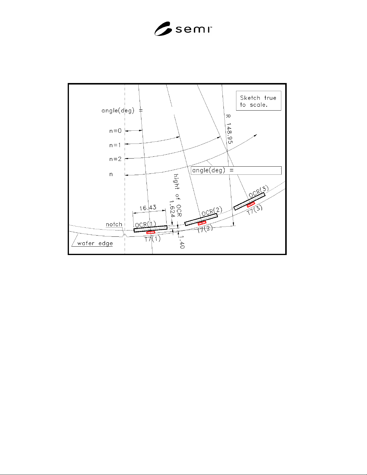
A1-5.1 Location of the Laser Inscription
A1-5.1.1 The original reference point shall be located
148.95 mm 0.15 mm from the center of the wafer
along a radius at 5.0 0.1 counterclockwise from the
axis of the fiducial bisector.
A1-5.1.2
The first re-inscription shall be placed
counterclockwise to the original mark at the same
distance from the wafer center on a radius 10
counterclockwise from the original mark.
A1-5.1.3 Any subsequent re-inscription shall be placed
counterclockwise to the previous mark at the same
distance from the wafer center on a radius 10
counterclockwise from the previous mark.
A1-5.1.4 Consequently, the most recent re-inscription
is located on a radius an angle
degrees
counterclockwise from the fiducial bisector as follows
(see Figure A1-1):
1.00.100.5
n
(1)
where
n = the total number of re-inscriptions.
SEMI M38-1104 © SEMI 1999, 2004 11
A1-5.2 Maintaining Inscription Utility — The angle of the new inscription shall be provided to the customer by the
supplier so that the tool used to read the inscriptions can be adjusted to read the wafer ID at the new angle. Since it
is possible for a tool to be provided the wrong angle to read an inscription, as long as the information remains the
same as the prior inscription, errors can be minimized (read attempts at different angles).
5° + n × 10°
5°
15°
25°
5° + n × 10°
Figure A1-1
Locations of Original Inscription and Subsequent Re-inscriptions on Back Surface of
Notched 300 mm Diameter Reclaimed Wafer