semi合集-English.pdf - 第5257页
SEMI M41-1101 © SE MI 2000, 2001 14 MHz frequen cy, 5 nm vo id gap and 50 µm void diameter can be detect ed. NOTE 16: Void is defined as “empt y space” th at is d ue to the impe r fect bon ding at Si/SiO 2 and Si O 2 / S…

SEMI M41-1101 © SEMI2000, 200113
Examples:
For Cu; HF-H
2
O
2
(HF : H
2
O
2
: H
2
O = 1 : 17 : 82)
For Au and Pt; aqua regia (HNO
3
: HCl = 1 : 3)
8.4.4 ICP-MS (Inductively Coupled Plasma Mass
Spectrometry) — ICP-MS is composed of ICP
(Inductively Coupled Plasma) part as an ion source and
MS (Mass Spectrometer) part, which measures the ions
generated at ICP part. Usually, sample solution is
vaporized in the nebulizer and then finally introduced
into Argon plasma in the silica tube called torch
through the spray chamber. The sample is decomposed,
evaporated, atomized and then ionized in the Argon
plasma. Except for few atoms that have relatively high
ionization potential, most of the elements (> 90%) can
be ionized. Ions are identified and measured in amount
by the mass spectrometer.
8.4.4.1 Sample Preparation — The same method as
AAS method is applicable. In case of quantitative
measurement of Fe, since its mass weight is close to
that of ArO
+
, it is necessary to pay attention to the
degradation of detection sensitivity.
8.5 Particle Density (LPD : Light Point Defect )
8.5.1 Light Scattering Tomography — The particle
larger than 0.2 µm on the thick SOI wafers is counted
by Automated particle counter. The particles in the
order of 0.1 µm can be detected if top silicon film is
sufficiently thick.
8.5.2 Principle of measurement — By scanning the
laser beam on the wafer surface, the light scattered by
the particles on the wafer is detected. The scattered
light and the noise from the wafer surface is detected as
a direct current, on the other hand, the scattered light by
the particles can be detected as pulse components. The
particle size can be calibrated with standard polystyrene
latex spheres. Multi-layers of SOI wafers usually have
scattering noise from the layer interface. In case of less
than 1 µm of the top silicon film thickness, it is
necessary to reduce incident angle of the laser beam to
increase the reflective component from the surface. For
example, S/N ratio is improved when using S-polarized
light of 10 degree incident, 85% of its component is
reflected from silicon surface.
NOTE 9: In case of SOI wafer (Thickness > 1 µm)
Particle counter with a vertical incident laser, which is the
same one used for the bulk wafer, is applied. It should be
noted that bypass filter to erase the interference signals due to
thickness dispersion, and adjustment of photo-multiplier
sensitivity are necessary. By this technique, it is capable of
detecting particles (> 0.1µm) as much as on the bulk wafer.
NOTE 10: In case of SOI wafer (Thickness < 0.5 µm)
It is recommended to use S - polarized light or normal light
with low incident angle because of high scattering noise.
However, the adjustment of photo-multiplier sensitivity is
necessary to reduce the noise component. The sensitivity
depends on the magnitude of the noise and it is usually
possible to detect particles of around more than 0.5µm (in
bulk wafer, > 0.2 µm).
8.5.3 Visual Inspection — SOI wafer can be visually
inspected in accordance with ASTM F523. The
automatic inspection equipment is also used when
available. For visual inspection, the collimated high
intensity bright light (ex. 500,000 lux) is used. Under
using this light, SOI wafer is inspected for haze, slip,
scratches, chips, cracks, pits, dimples, mound, orange
peel, LPD and contamination.
8.6 Surface Roughness
8.6.1 AFM (Atomic Force Microscope) — By
contacting the probe equipped with the cantilever onto
the wafer surface of the sample, and by scanning the
cantilever and detecting the variation by i.e., optical
method, the roughness information is obtained.
NOTE 11: It is expected to set the observation area as > 20
µm × 20 µm to increase reliability of the data.
NOTE 12: Height calibration of concave and convex: Refer to
UC standard (“Calibration method of 1 µm order height in
AFM”, [Ultra Clean Technology, Vol. 7, No. 2, pp. 43,
1995]).
8.7 Inclusions
8.7.1 In bonded SOI wafer, there exists the
contaminants at the bonding Si/SiO
2
or SiO
2
/SiO
2
interface such as particles, metals, boron, and
hydrocarbon. Here, inclusions means the contaminants.
Although there has been no report on the influence of
contaminants to the device characteristics, the
improvement of the contamination level is required.
8.8 Void
8.8.1 Scanning Acoustic Topography — The void can
be detected by means of the traveling time difference of
the acoustic waves. The void mapping can be made by
scanning an ultrasonic wave and detecting the reflecting
wave from the both surfaces of the void. Measuring in
water improves the resolving power of location since
the ultrasonic wave can be tightened by acoustic lenses.
NOTE 13: It is not suitable to measure SOI wafer that is not
bonded firmly because measurement is conducted in water.
NOTE 14: It is not suitable to measure top silicon film (< 7
µm) because it is impossible to separate reflective waves both
from top silicon film surface and the bonding interface.
NOTE 15: Detectable void gap depends on acoustic wave
frequency. Detectable void diameter depends on the size of
the acoustic source and the receiver. For example, if using 75
SEMI M41-1101 © SEMI 2000, 2001 14
MHz frequency, 5 nm void gap and 50 µm void diameter can
be detected.
NOTE 16: Void is defined as “empty space” that is due to the
imperfect bonding at Si/SiO
2
and SiO
2
/ SiO
2
interface. This
void should be discriminated from the splitting at bonding
strength test.
NOTE 17: Void can be only evaluated during SOI wafer
processing, not at the shipping.
8.9 Bonding Strength
8.9.1 Tensile Testing Method — Bonding strength is
defined and evaluated by tensile strength (kgf/cm
2
)
which is needed to split the bonding interface vertically.
Details of the test structure and the test method should
be determined by negotiation between wafer users and
wafer suppliers.
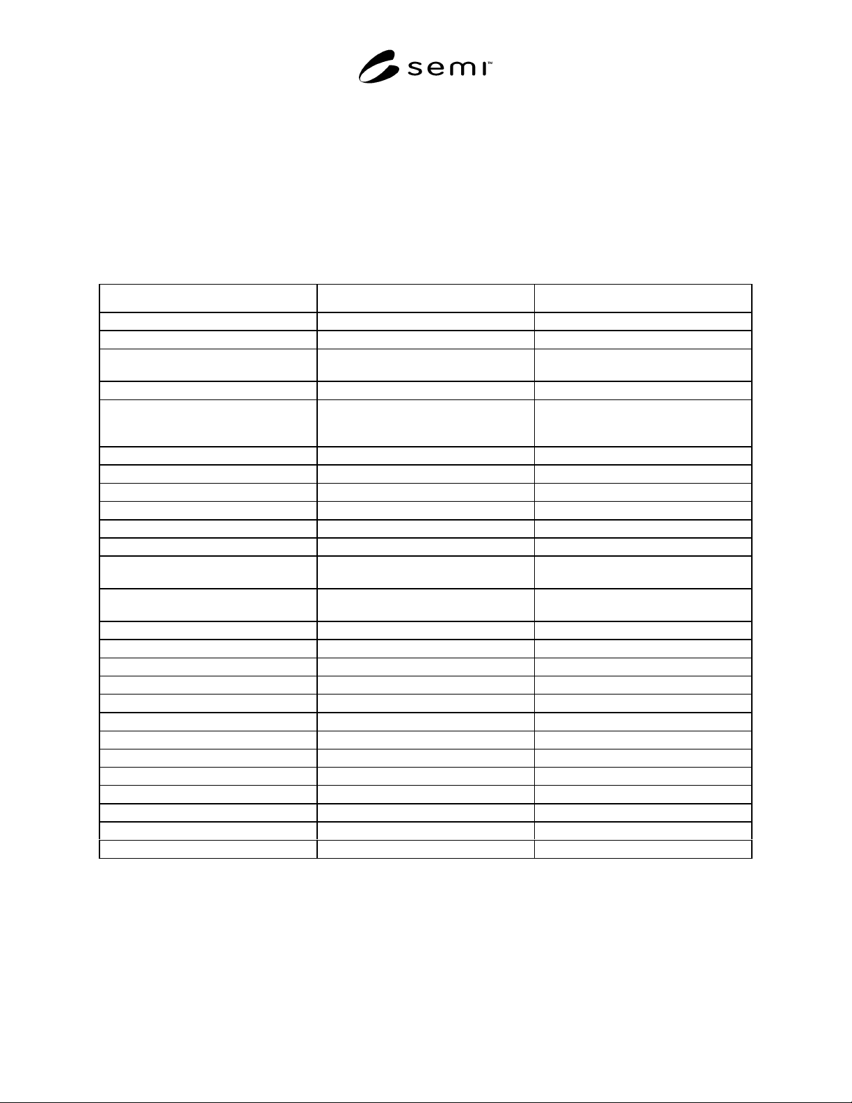
Table 6 Test Summary Table
Parameter Reference Method
Wafer Diameter F613-93 Optical Comparator
Wafer Thickness F533-96, F1530-94 Thick. Gage, Auto. Noncontact Scan.
Total Thickness Variation
LTV
F1530-94 Automated Noncontact Scanning
Warp F1390-92 Automated Noncontact Scanning
Crystal Orientation
Top Silicon Film (SOI)
Base Wafer
F26-87a (1993) X-ray Diffraction
Substrate Type / Dopant F42-93 Hot-Probe (Test Method A)
Substrate Resistivity F43-93, F84-93, F1527-94 4 Point Probe
Substrate RRG F81-95 4 Point Probe
Top Si Film Thickness Section 8.1 Reflective Spectroscopy or FTIR
Crystal Defect (OSF) Section 8.2, (JIS H 0609 :1994 B) Cr-free Etch / Optical Microscopy
Buried Ox defects Section 8.3, (SEMI M34) (a) Cu Decoration, (b) BOX Capacitor
Metal Contamination
(per unit area)
Section 8.4, (F1526-95) TXRF, AAS/ICP-MS
Particle Density ( LPD ) Section 8.5 (F1620-96) Light Scattering Tomography
( Automated Particle Counter )
Haze F523-93 (see NOTE 1), F154-94 Visual Inspection
Slip F523-93 (see NOTE 1), F154-94 Visual Inspection
Scratches F523-93 (see NOTE 1), F154-94 Visual Inspection
Chips / Cracks F523-93 (see NOTE 1), F154-94 Visual Inspection
Pits and Dimples F523-93 (see NOTE 1), F154-94 Visual Inspection
Mounds F523-93 (see NOTE 1), F154-94 Visual Inspection
Orange peel F523-93 (see NOTE 1), F154-94 Visual Inspection
Particle Density ( LPD ) F523-93 (see NOTE 1), F154-94 Visual Inspection
Contamination ( Both Side ) F523-93 (see NOTE 1), F154-94 Visual Inspection
Surface Roughness Section 8.6 AFM
Inclusions Section 8.7 SIMS
Voids Section 8.8 Scanning Acoustic Tomography
Bonding Strength Section 8.9 Tensile Strength
NOTE 1: Users and suppliers may agree on the non-SOI edge area for these specifications. For example the area within 6 mm proximity of the
wafer edge may be excluded.
SEMI M41-1101 © SEMI2000, 200115
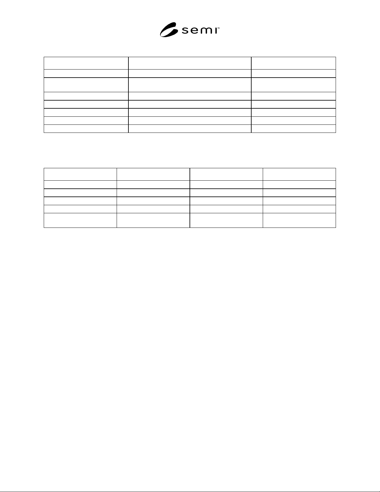
Table 7 Example: Soi Wafer Surface Visual Inspection Criteria
Criterion Items Allowed Quantity ( Per 150 mm Wafer ) Description
Haze NONE
Slip < 4
2 mm width and < 15 mm length
Scratches NONE
Chips / Cracks < 3 for @ 0.5 mm circumferential x 0.3 mm length Edge : Base Wafer
Pits and Dimples NONE
Particle Density ( LPD ) < 30 for @ > 0.2 µm <0.17 / cm
2
for 150 mm Wafer
Contamination NONE Both Surface and Backside
NOTE 1: The surface visual inspection is conducted under the collimated bright light.
NOTE 2: Non-SOI edge area (E.E. ) of 6 mm is applied to the criterion items except for edge chips/cracks.
NOTE 3: The whole wafer (Top silicon film and Base wafer) is inspected except for edge chips/cracks.
Table 8 Soi Electrical Parameters
Parameters Reference Value Method
Photo-conductivity Lifetime Section 9.1 To be determined µ-PCD
BOX Breakdown Section 9.2 To be determined I-V
BOX Charge Section 9.3 To be determined C-V
BOX Surface States Section 9.4 To be determined C-V
Doping Density
Top silicon film, Base wafer
Section 9.5 To be determined SIMS or 4 pt. probe
9 Electrical Parameters
9.1 Photo-conductivity Lifetime
9.1.1 Test Method:
µ-PCD method
9.1.1.1 Excess carriers that are created in the wafer by a light pulse increases the conductivity of the sample. When
the light is turned off, the conductivity is decreased by the carrier recombination. This phenom-enon is monitored
by means of microwave reflectance. The microwave detects an exponential decay in conduc-tivity, from which a
decay constant is determined.
9.1.2 The effective recombination lifetime τ
eff
is given by the following expression:
1/τ
eff
= 1/τ
B
+ 1/(τ
S
+ τ
D
)
τ
S
= d/(S
Si/Box
+ S
Si
), τ
D
= d/π
2
D
Where τ
B
is bulk recombination lifetime, τ
S
is surface recombination lifetime, τ
D
is diffusion lifetime, S
Si/Box
is
recombination velocity at the Box interface, S
Si
is recombination velocity at the silicon surface, D is diffusion
coefficient and d is top silicon film thickness.
9.1.3 The wavelength of the light has to be selected, depending on the top silicon film thickness (see Table 9).
9.2 Box Breakdown Voltage
9.2.1 Test Structure –– Box capacitor having an area (Ex. 1 cm
2
).
9.2.2 Test Method: Staircase I-V Measurement –– Voltage is stepwise increased in one-volt increments from zero to
the (+/-) specified voltage. Details of the test structure and the test method are determined by negotiation between
wafer users and wafer suppliers.
9.3 Box Charge
9.3.1 Test Structure — Box capacitor having an area (Ex. 1 cm
2
).