semi合集-English.pdf - 第5264页
SEMI M43-0301 © SE MI 2001 2 as bow, warp an d sori). This filtering may affect the reported results. 3.3 Nanotopography characterizat i o n does not in c lude microroughness, which applies to a shorter spatial wavel eng…

SEMI M43-0301 © SEMI 20011
SEMI M43-0301
GUIDE FOR REPORTING WAFER NANOTOPOGRAPHY
This guide was technically approved by the Global Silicon Wafer Committee and is the direct responsibility
of the North American Silicon Wafer Committee. Current edition approved by the North American Regional
Standards Committee on November 22, 2000. Initially available at www.semi.org December 2000; to be
published March 2001.
1 Purpose
1.1 This guide provides a framework for reporting of
nanotopography surface features on silicon wafers.
2 Scope
2.1 This guide addresses reporting the characterization
of nanotopography surface features found on wafer
surfaces. Nanotopography is the non-planar deviation
of the whole front wafer surface within a spatial
wavelength range of approximately 0.2 to 20 mm and
within the fixed quality area (FQA). Typical examples
include dips, bumps or waves on the wafer surface that
vary in peak to valley height from a few nanometers to
a several hundred nanometers.
2.2 This guide provides a framework for communi-
cating specific values limiting feature levels and/or
densities as agreed upon between suppliers and users.
2.2.1 Discussion — Nanotopography measurements
have not been needed for 0.25 µm generation devices,
but are expected to be required for smaller feature sizes
to meet CMP requirements. Nanotopography on a wafer
surface prior to CMP processes can result in variations
in post-CMP dielectric thickness with potential negative
consequences for circuit performance and yield;
features as small as 20 nm (peak to valley) can result in
post CMP discoloration of dielectrics as a result of local
thickness variation of the remaining dielectric
1
1
. Height
variations over specified distances (determined by CMP
issues and/or lithography systems) need to be properly
controlled to assure that wafers are acceptable for
selected process steps. In the case of CMP, the issue is
control of film thickness variation introduced by
nanotopography. The metrology industry is building
tools that will measure and map surface features at
nanotopography amplitudes and spatial wavelengths.
Nanotopography features are characterized by their
height variation within an area, and are discriminated
from other features of similar height by their spatial
wavelength range.
2.3 This standard does not purport to address safety
issues, if any, associated with its use. It is the
responsibility of the users of this standard to establish
1 K. V. Ravi, “Wafer Flatness Requirements for Future
Technologies,” Future Fab International, July 1999.
appropriate safety health practices and determine the
applicability or regulatory limitations prior to use.
3 Limitations
3.1 The reported surface features will be influenced by
limitations and parameters of the measurement tool.
These include:
3.1.1 The finite surface spatial bandwidth of the tool
and the applied filtering will prevent surface variations
outside the bandwidth of operation from being
measured. Also, the finite bandwidth of filtering
produces non-physical artifacts that may be apparent in
regions where the power in the rejected bands is high.
3.1.2 Bandwidth edges are not always well defined.
Measurement results do not always agree well between
systems, because different tool designs employ differ-
ent geometries and operate them over different spatial
bandwidths.
3.1.3 All surface profiling measurement systems have
a minimum height variation sensitivity that will distort
signals near the noise floor.
3.1.4 The reported shape of some features may also
depend on the pixel grid orientation employed by the
instrument.
3.1.5 The pixel size and sampled area will affect the
bandwidth limits.
3.2 Reported profiles also vary with interactions
between wafer and tool. These limitations include:
3.2.1 Measurements made near the wafer edge may
result in false readings. Under certain conditions, this
may cause incorrect height measurement within the
FQA.
3.2.2 Closely spaced features may be counted as a
single feature, or as no feature, if the pixel size is larger
than the feature, or is larger than the spacing between
features. Reported features may result from the
combination of the actual surface features, the manner
in which the wafer is chucked, or be caused by particles
trapped between the wafer back surface and the chuck.
3.2.3 High-pass (spatial frequency) filtering is
typically used with these measurements to remove the
(long-spatial wavelength) effects of wafer shape (such

SEMI M43-0301 © SEMI 2001 2
as bow, warp and sori). This filtering may affect the
reported results.
3.3 Nanotopography characterization does not include
microroughness, which applies to a shorter spatial
wavelength range.
3.4 The location of defective areas as calculated in
section 6 may not coincide with the location of the
surface features that lead to those values. This may
cause lack of spatial correlation between reported
defective areas and device process defect areas.
3.5 The height map used to create nanotopography
reports may be affected by wafer shape and
measurement chuck effects.
4 Referenced Standards
4.1 SEMI Standards
SEMI M1 Specification for Monocrystalline
Polished Silicon Wafers
NOTE 1: As listed or revised, all documents cited shall be the
latest publications of adopted standards.
5 Terminology
5.1 fixed quality area (FQA) [SEMI M1] — the
central area of a wafer surface, defined by a nominal
edge exclusion, X over which the specified values of a
parameter apply.
Discussion: The boundary of the FQA is at all points
the distance X away from the periphery of a wafer of
nominal dimensions. (See Figure 1). The size of the
FQA is independent of the wafer diameter and flat
length tolerances. For the purpose of defining the FQA,
the wafer periphery at locations with notch fiducials is
assumed to follow the circumference of a circle with
diameter equal to the nominal wafer diameter.
5.2 nanotopography, of a wafer su rface — the non-
planar deviation of a surface within a spatial
wavelength range of approximately 0.2 to 20 mm.
5.3 nanotopology, of a wafer surface — see
nanotopography.
5.4 roughness [SEMI M1] — the more narrowly
spaced components of surface texture.
Discussion: These components are considered within
defined limits of spatial wavelength (or frequency).
5.5 spatial wavelength — the spacing between
adjacent peaks of a purely sinusoidal profile.
6 Measurements
6.1 The height map is obtained from a front-surface
measurement. An explicit reference plane is not used
for calculating and assigning values.
NOTE 2: Other methods of analyzing nanotopography may
require the use of an explicit reference plane.
6.2 The high-pass filter removes long spatial
wavelength wafer tilt and topography effects,
effectively creating a global reference surface.
6.3 Calculation — The calculation determines the
peak to valley height (P-V) variation among the pixels
included in the analysis area, and assigns that variation
in nanometers to the center of the analysis area. The
calculation is performed for every analysis area within
the FQA of the wafer. These calculations may be
repeated for analysis areas of different dimension D.
NOTE 3: This calculation describes the “full-analysis area”
method. There is another calculation, the “partial analysis
area” method, where the calculation is performed for every
analysis area whose center pixel is within the FQA of the
wafer. The partial analysis area method, not defined in this
document, is being addressed by SEMI for inclusion in a
standard.
6.4 The following measurement elements should be
reported:
6.4.1 Filtering
a) Spatial cutoff of high pass filter
b) Type of Filter
c) Pixel spacing
Filtering is used to remove long wavelength shape
components from the raw height data.
6.4.2 Analysis Area — Specify this analysis area’s:
a) Shape, e.g., square, circle, and
b) Dimension D of the analysis area
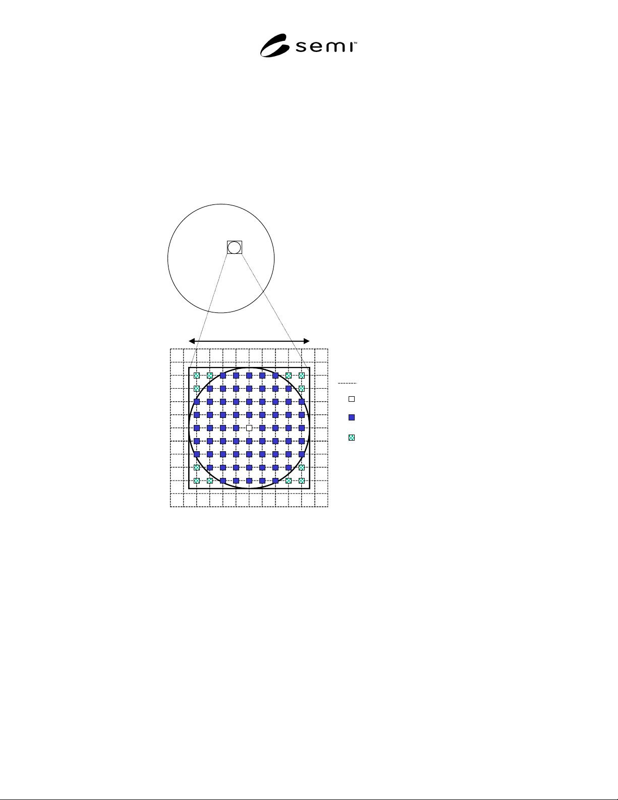
An analysis area contains a pixel at its center (Figure
1). The pixels within the surrounding analysis area of
dimension D, and within the FQA, are used to deter-
mine the value assigned to the center pixel location.
6.4.3 Data Report — Report one or more of the
following:
6.4.3.1 Statistical Representation by Threshold Curve
— Plot, for each D, % area vs. threshold T, in
nanometers, where % area is the ratio of
a) the number of analysis areas whose assigned value
(calculated per Section 6.3) exceeds the threshold
T, to
b) the number of pixels within the FQA.
The ratio is expressed as a percentage.
SEMI M43-0301 © SEMI 20013
6.4.3.2 Tabular Representation by % Area Sorted — Specify a threshold T for each D and report the % area.
6.4.3.3 Tabular Representation by Threshold — Specify a % area for each D and report the Threshold, T.
6.4.3.4 Spatial Representation by Height Map — Generate a whole wafer height map of the surface.
6.4.3.5 Spatial Representation by Defect Map — Generate a whole wafer height map of the surface. Analysis areas
whose assigned values (calculated per Section 6.3) exceed the threshold in Section 6.4.3.2 are flagged for each D.
6.4.3.6 Spatial Representation by PV Analysis Map — Generate a whole wafer map of the values assigned in
Section 6.3.
Pixel grid center lines
Center pixel, included
Included pixels
Included pixels, square
D
Pixel grid center lines
Center pixel, included
Included pixels
Included pixels, square
D
Figure 1
The Analysis Area Of Dimension D, Center And Included Pixels Are Indicated
NOTICE: SEMI makes no warranties or representations as to the suitability of the standard set forth herein for any
particular application. The determination of the suitability of the standard is solely the responsibility of the user.
Users are cautioned to refer to manufacturer’s instructions, product labels, product data sheets, and other relevant
literature respecting any materials or equipment mentioned herein. These standards are subject to change without
notice.
The user’s attention is called to the possibility that compliance with this standard may require use of copyrighted
material or of an invention covered by patent rights. By publication of this standard, SEMI takes no position
respecting the validity of any patent rights or copyrights asserted in connection with any item mentioned in this
standard. Users of this standard are expressly advised that determination of any such patent rights or copyrights, and
the risk of infringement of such rights, are entirely their own responsibility.