semi合集-English.pdf - 第5295页
SEMI M48-1101 © SEMI 2001 5 R 1 = 0.10 mm an d θ 1 = 0.52°. Successive points are incremented with ∆ R = 1.21 m m and ∆ θ = 1.16°. NOTE 5: Spiral scans un iformly sample properties that are radially symmetrica l. These s…

SEMI M48-1101 © SEMI 2001 4
6.4.2 Record final film thickness in the same locations
employed for the starting film.
6.4.3 Calculate global and local film thickness changes
appropriate for the application of interest.
6.5 Metrology tools
6.5.1 Select a film thickness measurement system
suitable for the film and sampling pattern to be
characterized.
6.5.1.1 Perform a gauge study on each metrology tool
accordance with SEMI E89 to determine its
effectiveness for the films to be measured.
6.5.2 Ascertain that the metrology tool is operating
properly under Statistical Process Control prior to use
in the CMP process test.
6.5.3 Perform tool calibration in accordance with the
tool supplier’s instructions.
6.6 CMP Consumables
6.6.1 Identify all consumables including pad, insert
film, slurry type, and conditioning end effector.
6.6.2 Record the manufacturer’s part number and lot
number (if available) of each consumable item.
6.6.3 Record the status and history of each consumable
prior to starting the process test.
NOTE 3: The history of consumables can affect the CMP
process test.
6.6.4 Perform break-in procedures for pad and carrier
film as required to ensure stable operation. Base these
break-in procedures on recommendations from the
consumable supplier.
6.7 Polishing Tool
6.7.1 Calibrate and record polish downforce, alignment
tolerances, velocity, fluid dispense rates and other
operational parameters based on recommended
procedures from the equipment manufacturer.
6.7.2 Polish the samples.
7 Measurement Locations on the Wafer
7.1 The number and location of measurement sites are
specific to the process test. In general, locations should
be evenly spaced. Data extrapolation beyond the
boundary of the measurement site population should
not be performed.
7.2 ASTM F 1618 covers a set of site distribution
patterns for measuring the uniformity of a thin film on a
silicon wafer, similar to Figures 2 – 5, as well as simple
procedures for analyzing and reporting the results of
those measurements. For edge-scan measurements, see
Section 7.3.6 below. For spiral-scan measurements, see
Section 7.3.7 below. For full-wafer, high-density
measurements, see Section 7.3.10 below.
7.3 Select one of these patterns for CMP process
analysis on unpatterned wafers, unless otherwise agreed
to.
7.3.1 Sampling plans are based on concentric circles,
spirals, Cartesian sites, partial-radius, and partial and
single-diameter sites.
7.3.2 Measurements are made at the sites specified in
the chosen sampling plan, using the appropriate
instrumentation and measurement procedure for the
film parameter of interest.
7.3.3 Measures of the dispersion of the values are
obtained by simple statistics specified for the sampling
plans.
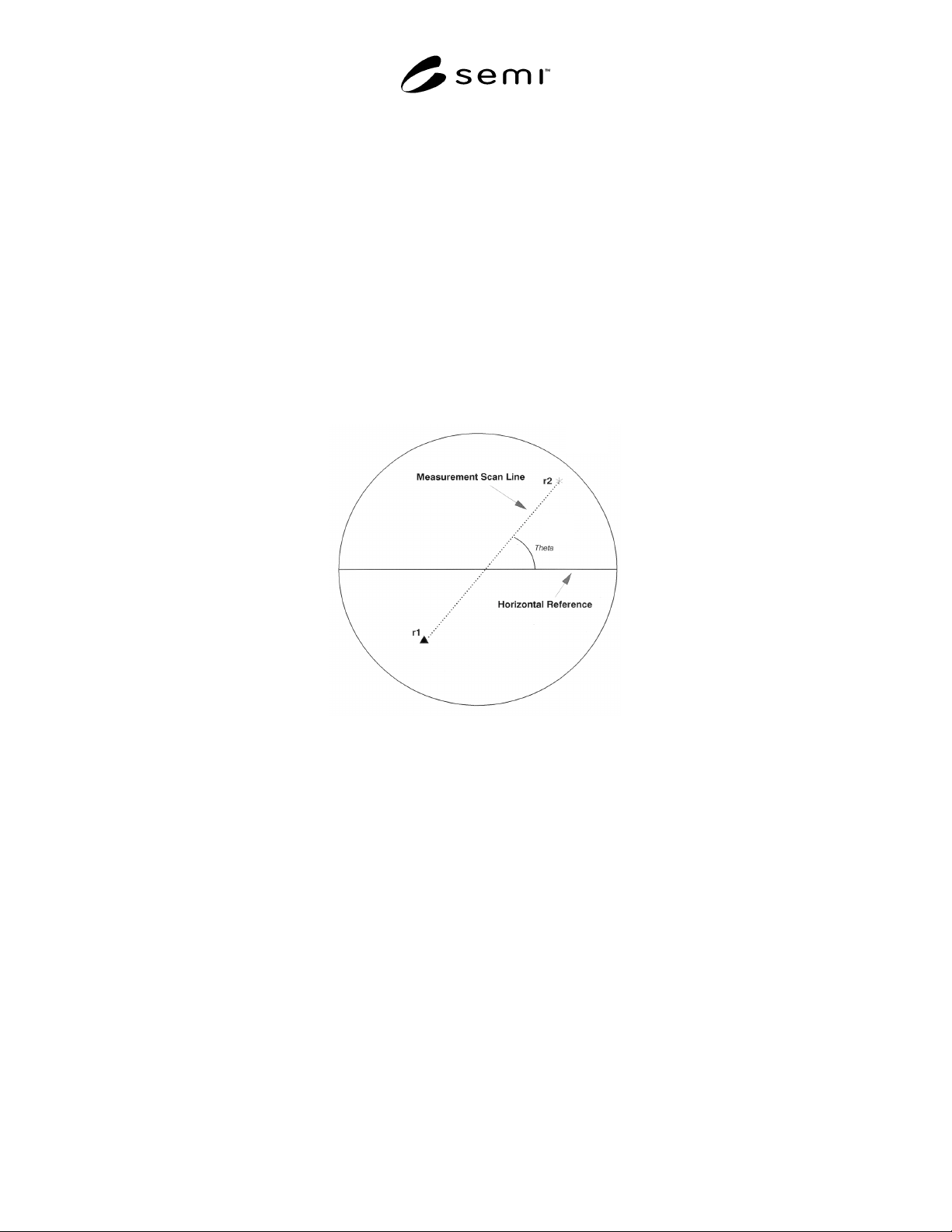
7.3.4 For diagonal scan measurements, refer to Figure
1. Select values for each of the following scan
parameters:
• Scan Angle,
θ
• Scan Radius Start/Stop, r
1
/ r
2
• Number of Measurement Points, n, across the
diameter.
7.3.5 For edge scan measurements, refer to Figure 6.
Select values for each of the following scan parameters:
• Scan Angle,
θ
• Inner Scan Radius, r
1
• Outer Scan Radius, r
2
• Number of Measurement Points, n, between r
1
and
r
2
.
NOTE 4: These n measurement sites are uniformly
distributed.
7.3.5.1 Discussion — the data density for edge scan
measurements is generally higher than for other
measurements. Combining a low-density diameter
scan in the central region of the wafer with a higher-
density edge scan, taken along the same scan line, can
improve throughput with appropriate local
measurement data density.
7.3.6 For spiral scan measurements, refer to Figure 7.
In such scans, the measurements are evenly distributed
from near the center (r = 0) to near the edge exclusion
boundary (r = 1 – EE). For each successive point, both
the radius and the angle
θ
are systematically changed.
For the 200 mm example with 3 mm edge exclusion
shown in Figure 7, the 81 measurement points start at
SEMI M48-1101 © SEMI 2001 5
R
1
= 0.10 mm and
θ
1
= 0.52°. Successive points are
incremented with ∆R = 1.21 mm and ∆
θ
= 1.16°.
NOTE 5: Spiral scans uniformly sample properties that are
radially symmetrical. These scans apply equal weight to all
measurement sites. They also provide radial information,
similar to diameter scans, as well as additional theta-related
information that may not be provided by diameter scans.
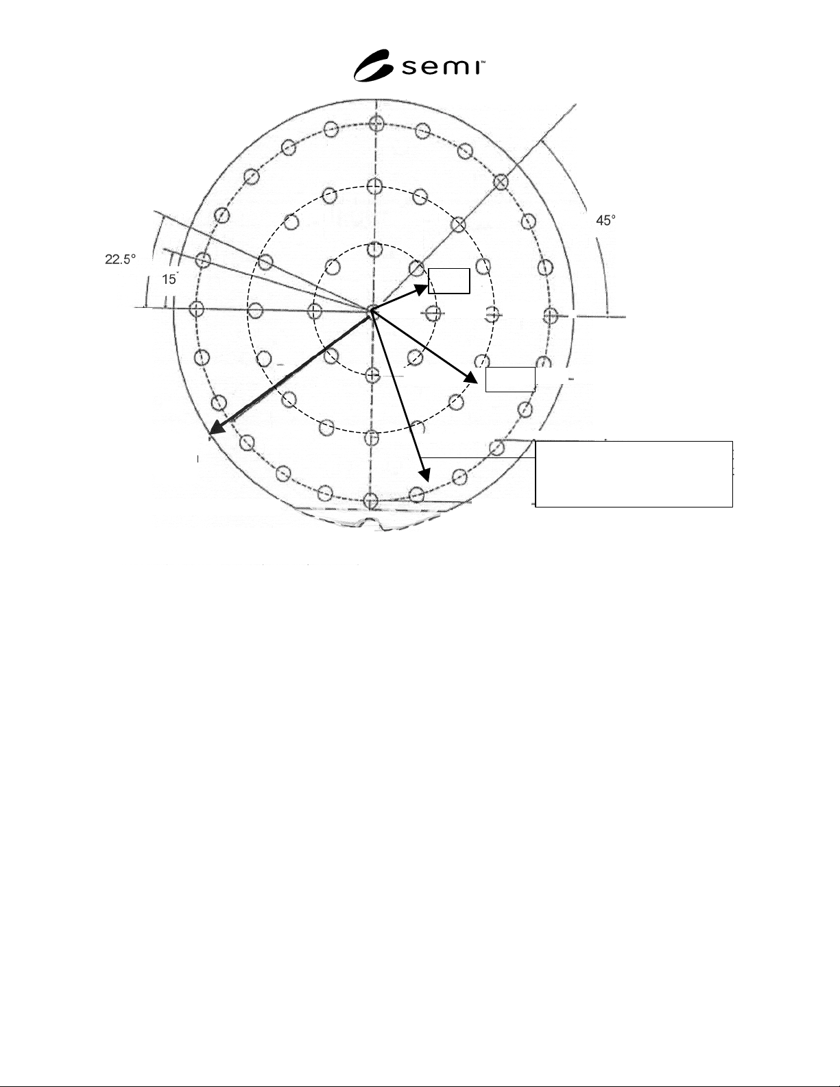
7.3.7 For concentric circle scans, refer to Figures 2 and
3. In these scans, the inner circles lie on a fraction of
the nominal radius. For notched wafers, the outer circle
lies on a radius equal to the nominal radius less the
edge exclusion, which is conformal with the notch on
notched wafers. For flatted wafers the outer circle lies
on a radius equal to the nominal radius less the sum of
the flat depth plus the edge exclusion.
7.3.8 For Cartesian measurement scans, refer to Figure
4.
7.3.9 For full-wafer measurements, the measurements
sites are evenly spaced over the entire area being
examined. Typically, the first point is the wafer center,
and the remaining measurement sites are equally spaced
about the wafer center in X and Y. This X-Y grid is
similar to Figure 4, but with significantly higher spatial
density.
7.4 Record and identify the measurement site locations
in accordance with SEMI M20.
7.4.1 Include an illustration of these locations with the
test setup and with the recorded data set.
θ
Figure 1
Diameter Scan
θ
= scan orientation; r
1
, r
2
= scan start/stop
SEMI M48-1101 © SEMI 2001 6
R/3
Notched Wafers = R
nom
– EE
Flatted Wafers = R
nom
– (EE
+ Flat Depth)
R
nominal
2R/3
°
Figure 2
Three Concentric Circles