semi合集-English.pdf - 第5296页
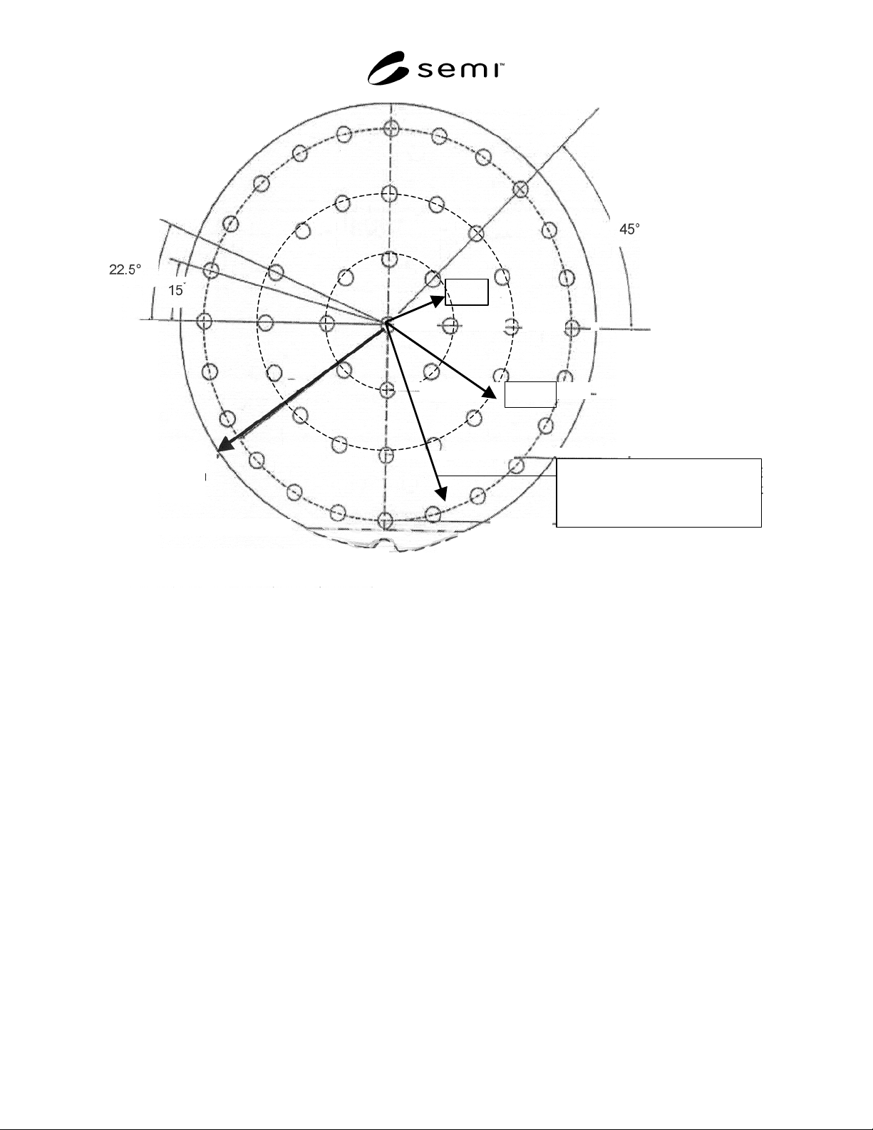
SEMI M48-1101 © SEMI 2001 6 R/3 Notched W afers = R nom – EE Flatted W afer s = R nom – (EE + Flat De pth) R nominal 2R/3 ° Figure 2 Three Concentric Circles
SEMI M48-1101 © SEMI 2001 5
R
1
= 0.10 mm and
θ
1
= 0.52°. Successive points are
incremented with ∆R = 1.21 mm and ∆
θ
= 1.16°.
NOTE 5: Spiral scans uniformly sample properties that are
radially symmetrical. These scans apply equal weight to all
measurement sites. They also provide radial information,
similar to diameter scans, as well as additional theta-related
information that may not be provided by diameter scans.
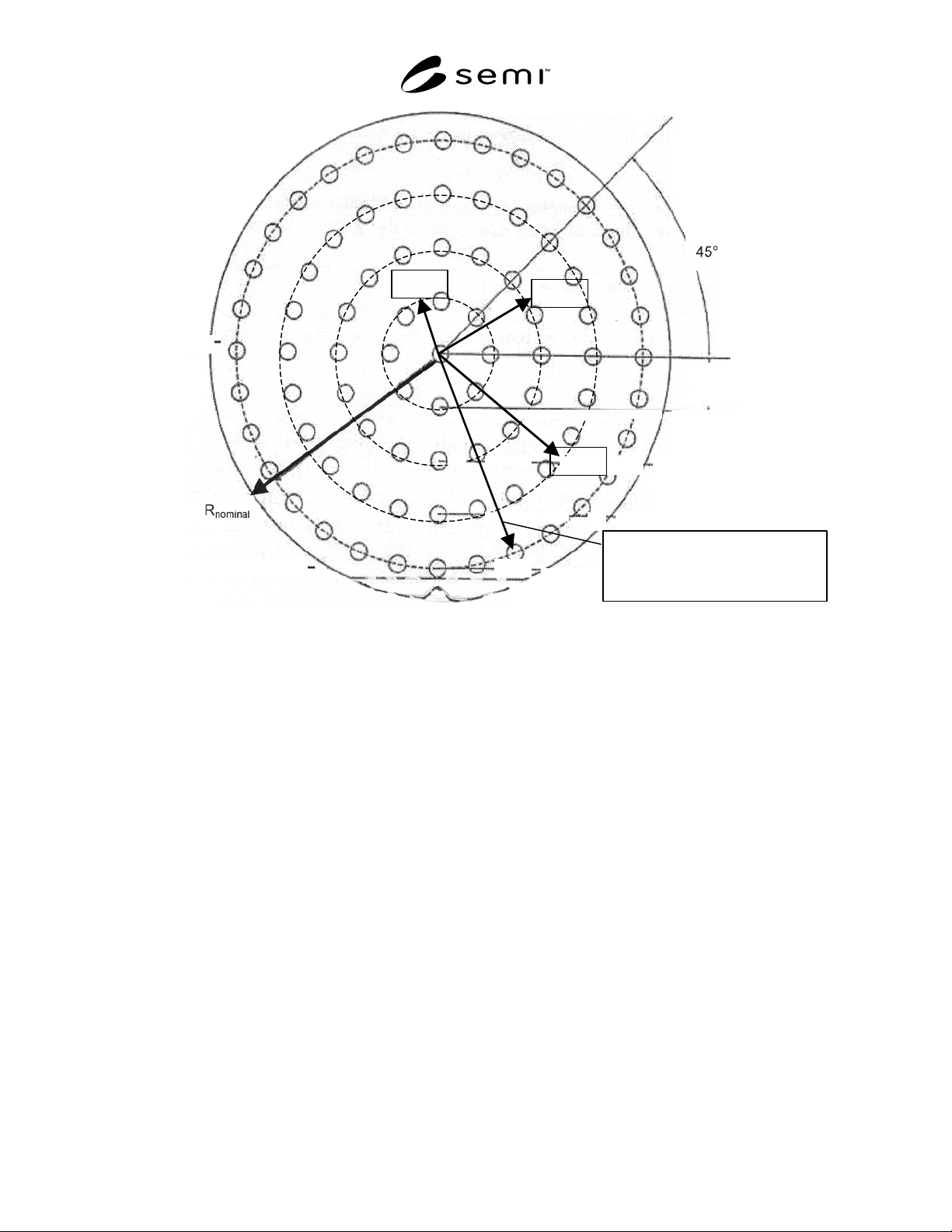
7.3.7 For concentric circle scans, refer to Figures 2 and
3. In these scans, the inner circles lie on a fraction of
the nominal radius. For notched wafers, the outer circle
lies on a radius equal to the nominal radius less the
edge exclusion, which is conformal with the notch on
notched wafers. For flatted wafers the outer circle lies
on a radius equal to the nominal radius less the sum of
the flat depth plus the edge exclusion.
7.3.8 For Cartesian measurement scans, refer to Figure
4.
7.3.9 For full-wafer measurements, the measurements
sites are evenly spaced over the entire area being
examined. Typically, the first point is the wafer center,
and the remaining measurement sites are equally spaced
about the wafer center in X and Y. This X-Y grid is
similar to Figure 4, but with significantly higher spatial
density.
7.4 Record and identify the measurement site locations
in accordance with SEMI M20.
7.4.1 Include an illustration of these locations with the
test setup and with the recorded data set.
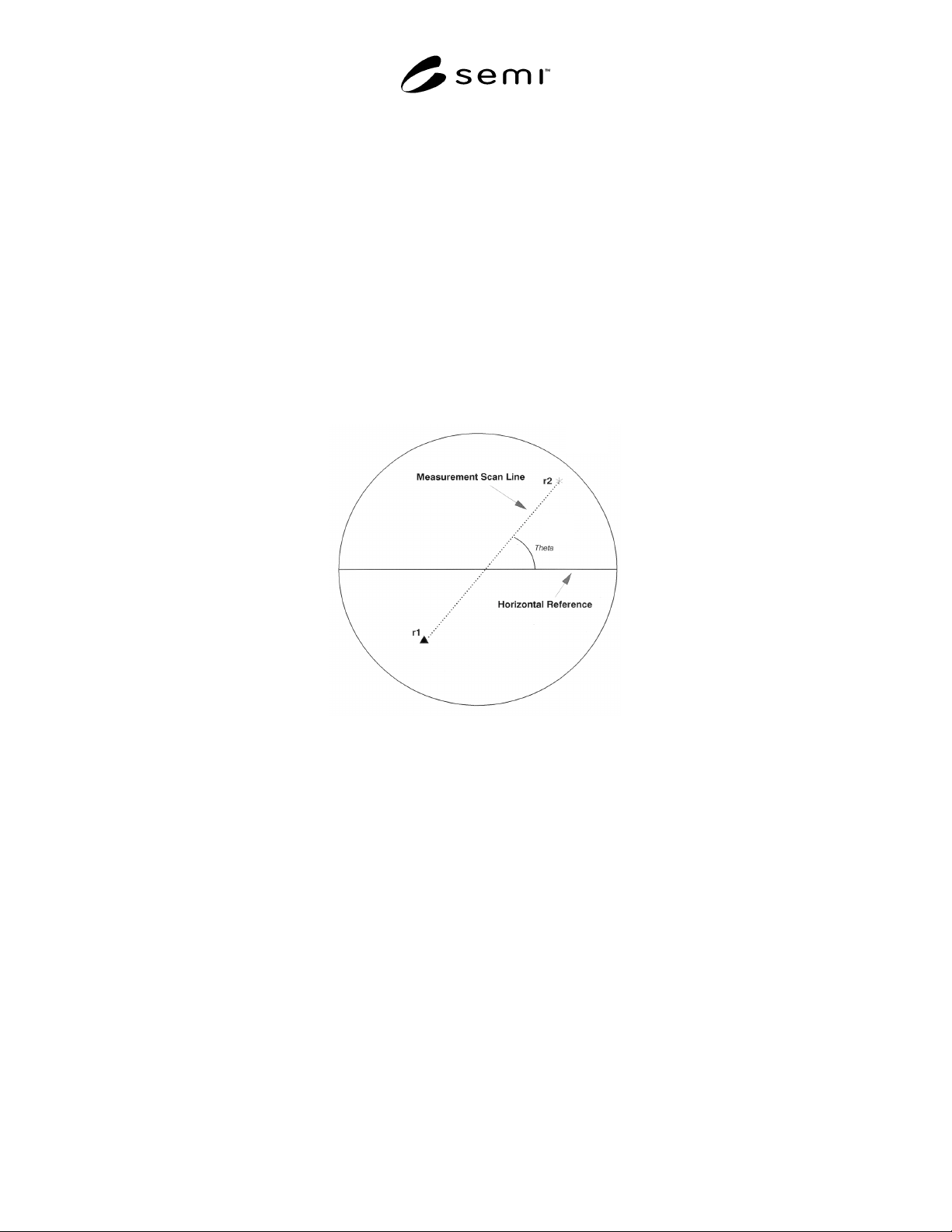
θ
Figure 1
Diameter Scan
θ
= scan orientation; r
1
, r
2
= scan start/stop
SEMI M48-1101 © SEMI 2001 6
R/3
Notched Wafers = R
nom
– EE
Flatted Wafers = R
nom
– (EE
+ Flat Depth)
R
nominal
2R/3
°
Figure 2
Three Concentric Circles
SEMI M48-1101 © SEMI 2001 7
Notched Wafers = R
nom
– EE
Flatted Wafers = R
nom
– (EE
+ Flat Depth)
R/4
3R/4
R/2
Figure 3
Four Concentric Circles