semi合集-English.pdf - 第5327页
SEMI M51-0303 © SEMI 2002, 2003 5 some of the proper C-mode events in which the gate oxide was not br oken down are counted B-m ode failures. Both cases will be taken as a mistake in the classification of the failure mod…

SEMI M51-0303 © SEMI 2002, 2003 4
resisitivity is too low, the gate oxide dielectric characteristics
degrade. Too thin a polysilicon electrode makes self-healing
of oxide weak spots easier. This self-healing causes the oxide
breakdown defect density to be underestimated. Too thin
polysilicon electrode also causes the TZDB measurement to
be degraded by mechanical stress resulting from an exploring
probe such as a tungsten probe. With too thick of a
polysilicon electrode in the ex-situ doping technique, it is easy
to induce a depletion layer of phosphorus near the
polysilicon/SiO
2
interface that causes parasitic resistance and
unnecessary voltage drop in the measurement circuit. It is
desirable to monitor the thickness and sheet resistance of the
polysilicon layers in every processing batch using a monitor
wafer.
5.2.7 Photolithography Process — The MOS
capacitors electrodes are formed by patterning in the
photolithography. EIA/JEDEC Standards 35, 35-1, 35-2
are referred to regarding this mask design. The
appropriate area and the appropriate number of MOS
capacitors for each defect density shall be selected in
order to detect crystal defects. For the evaluation of
COPs, it is necessary to measure 100 or more MOS
capacitors with a gate area of about 10 mm
2
on a wafer.
(See Table R1-3 in Related Information 1.) For spares,
it is desirable to prepare the plural MOS capacitors with
the same gate area within each chip.
5.2.8 Etching Processes — The photo resist pattern
formed by the photolithograph technique is used as a
mask for polysilicon etching. Generally, either a wet
etching method or a dry etching method is applied to
polysilicon etching. If a wet etching method is applied,
the etching rate shall be well controlled. If the
peripheral oxide of the electrode is removed, it is
sometimes difficult to accurately measure the TZDB. If
a dry etching method is applied, especially RIE, care
shall be taken with the charging-up of the MOS
capacitors. In cases where the A-mode defect density is
high, the MOS capacitors shall be confirmed not to be
charged up during the etching process. If an ashing
removal is carried out with the photo resist, care shall
be taken with the charging-up of the MOS capacitors.
As with RIE, in cases where the A-mode defect density
is high, the MOS capacitors shall be confirmed not to
be charged up during the ashing removal process. If
there are oxide and polysilicon film on the backside of
the wafer, those shall be removed.
5.3 Measurement of the Electrical Characteristics of
MOS Capacitors
5.3.1 The dielectric breakdown defect density of
silicon oxide is evaluated by the TZDB method for
MOS capacitors. In the TZDB method, the gate oxide
electric field of an MOS capacitor is continuously
increased in stepwise fashion. The electric field applied
to the gate oxide when the gate oxide leakage current
exceeds the predetermined dielectric breakdown
judgment value is defined as the oxide dielectric
breakdown field. From a histogram of the breakdown
fields for 100 or more MOS capacitors, the dielectric
breakdown defect density is estimated.
5.3.2 We can see two characteristics of the formed
MOS capacitors from the current-voltage (I–V) plots.
Firstly, deviation of the gate oxide thickness appears in
a loose distribution of the I-V plots. Secondly, if the I-
V curves bend suddenly and have gentle slope in the
high voltage region, there may be high parasitic
resistance, for example, high resistance in the
polysilicon electrode. In such a case, the reliable
measurement demands the adjustment of the MOS
preparation process.
5.3.3 Applied Step Voltage
NOTE 8: For a reliable measurement, a voltage source with
a well-defined output shape shall be used. An overshooting
of the applied step voltage decreases the apparent oxide
breakdown voltage as compared with a real breakdown
voltage. In the TZDB measurement, the constant voltage is
held after a predetermined period and the oxide leakage
current is measured. Next, the applied voltage increases
stepwise. This procedure is repeated. If the holding time is
shorter than 100 ms, the voltage may not be stable enough to
allow the current to be measured. 800 ms may be enough to
achieve a stable voltage. Especially, in the high electric field
region, the gate oxide may receive electric stress similar to
time dependent dielectric breakdown (TDDB). A holding
time of 200 ms is recommended. Accordingly to the round
robin result as described in Related Information 1, there are
no problems in setting the holding time to 100–800 ms. The
recommended step height of the applied voltage is between
0.1–0.5 MV/cm in electric field. The polarity of the voltage is
selected for the Si surface so as to be in accumulation. That
is, for p-type silicon wafers, the gate electrodes are negatively
biased. The maximum electric field is 15 MV/cm. Even if a
gate voltage corresponding to more than 15 MV/cm is
applied, the voltage is not effectively applied to the gate oxide
because of a voltage drop due to parasitic resistance. In the
case of n-type silicon wafers, the applied electrodes shall be
positively biased.
5.3.4 Breakdown Judgment
5.3.4.1 The oxide dielectric breakdown is judged by
the predetermined oxide leakage current. That is, when
the gate oxide leakage current exceeds the dielectric
breakdown judgment current, the applied voltage is
defined as the breakdown voltage. The breakdown
electric field is the value that the breakdown voltage is
normalized by the gate oxide thickness.
5.3.4.1.1 Discussion — If the dielectric breakdown
judgment current is too high (Ig > 10
–3
A), some of the
proper A-mode failures can be counted as B-mode
failures because of the series resistance of the samples
or measurement system. Otherwise, if the dielectric
breakdown judgment current is too low (Ig < 10
–7
A),
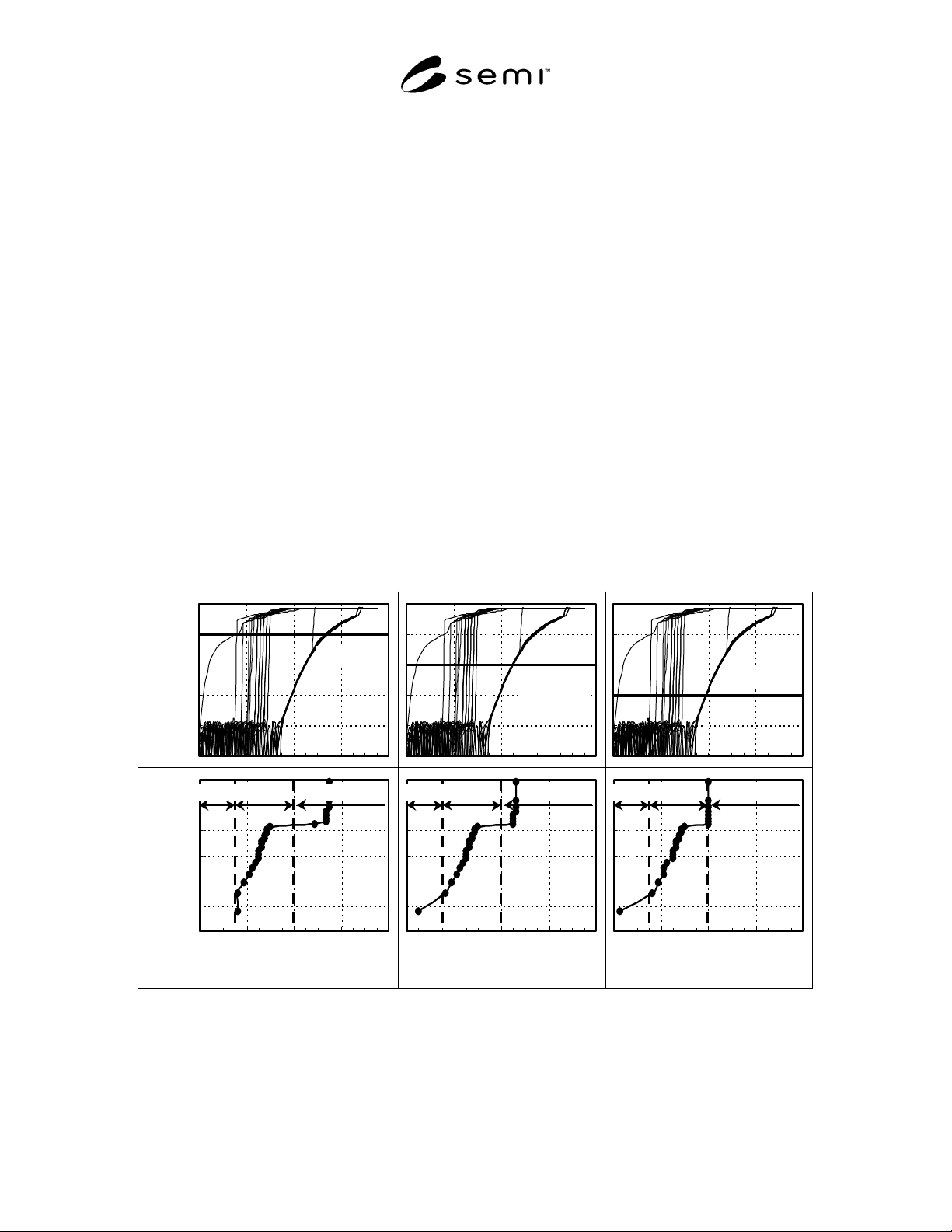
SEMI M51-0303 © SEMI 2002, 2003 5
some of the proper C-mode events in which the gate
oxide was not broken down are counted B-mode
failures. Both cases will be taken as a mistake in the
classification of the failure modes, even if the
measurement is accurately done and the appropriate I-V
curves measurements are achieved. A dielectric
breakdown judgment current of 10
–5
A is
recommended.
6 Significance and Use
6.1 This standard gives instructions of the procedure
for characterizing mirror-polished, p-type CZ silicon
wafers by measuring the dielectric breakdown defect
density in the thermally grown gate oxide film using the
MOS capacitors. The MOS capacitors must be formed
in accordance with the fabrication process described in
Section 5 that influences the oxide characteristics.
6.2 It is well known that both the silicon surface
morphology and the cross-sectional structure at the
pattern edge of the active region of the MOS devices
influences the dielectric breakdown of the gate oxide.
Various kinds of contaminations also influence the
dielectric breakdown of the gate oxide. Contamination
by alkaline or heavy metals and organic particles
increases as the sample fabrication process progresses.
Furthermore, COPs increase with increasing SC-1
treatment. These facts indicate that it is desirable to
simplify the sample structure and its fabrication
processes to characterize a silicon wafer by TZDB of
the gate oxide. Thermal processes can cause growth of
oxygen precipitates in a silicon wafer. This standard
cannot be applied to silicon wafers that might receive
such thermal processes.
6.3 The appropriate area and the appropriate total
number of the tested MOS capacitors shall be chosen so
as to answer the purpose of this standard test. For
example, as shown in Table R1-3, it is suitable to select
a gate electrode area of 10 mm
2
and a total number of
capacitors of more than 100.
6.4 The electrode material of the MOS capacitors has a
great influence on the dielectric breakdown of the gate
oxide. Polysilicon is specified as the electrode material
in this standard. It is applied to practical ultra large-
scale integrated circuits (ULSI). The polysilicon
electrode yields test results highly consistent with the
actual ULSI performance.
1E-11
1E-9
1E-7
1E-5
1E-3
1E-1
0 4 8 12 16
Ebd (MV/cm)
Current (A)
Ig > 1E-7 A
-4
-3
-2
-1
0
1
2
0481216
Ebd (MV/cm)
(ln(-ln(1-P)))
B-mode C-mode
A
-mode
Ig > 1E-3 A Ig > 1E-5 A Ig > 1E-7 A
1E-11
1E-9
1E-7
1E-5
1E-3
1E-1
0 4 8 12 16
Ebd (MV/cm)
Current (A)
Ig > 1E-5 A
-4
-3
-2
-1
0
1
2
0481216
Ebd (MV/cm)
(ln(-ln(1-P)))
B-mode C-mode
A
-mode
1E-11
1E-9
1E-7
1E-5
1E-3
1E-1
0 4 8 12 16
Ebd (MV/cm)
Current (A)
Ig > 1E-3
A
-4
-3
-2
-1
0
1
2
0481216
Ebd (MV/cm)
(ln(-ln(1-P)))
B-mode C-modeA-mode
Figure 1
Comparison of Judgment Conditions

SEMI M51-0303 © SEMI 2002, 2003 6
7 Interferences
7.1 Since this is a DC measurement, care must be taken
to make sure that the silicon wafer has a low resistance
ohmic contact. There must be no dielectric film on the
back surface, e.g. silicon oxide, in order to effectively
apply a voltage bias to the gate oxide. It is not
necessary for this to be done with a metallic contact to
the back surface of the wafer under test.
7.1.1 However, when the vacuum chucking is weak,
care must be taken because of the possibility that the
dielectric breakdown voltage of the gate oxide is not
accurately measured due to an increase in parasitic
resistance.
7.2 It is strongly suggested that testing be done with a
voltage polarity such that the silicon surface will be in
accumulation below the gate oxide, that is, negative
voltages for p-type silicon wafers. If the polarity of the
voltage is chosen to be in the reverse direction, the
breakdown voltage may not be accurately measured due
to the presence of a depletion layer below the gate
oxide.
7.3 Evaluation and control of electrical noise in the
current-voltage data, as part of this test method are
crucial to the proper identification of the failure criteria.
7.4 In the TZDB measurement, lowering of the
electrical noise under a low bias stress condition is
made possible by the averaging of measurement data.
While the required 100 ms holding time may be set
using a delay in the measurement loop, an additional,
uncontrolled delay may be incurred due to the
autoranging of an electrometer. The effect is most
pronounced for very low oxide leakage currents, where
the measured value is several orders of magnitude
below the minimum range set by the electrometer
software.
7.5 Mechanical stress by the exploring probe can
influence the measurement results, because the
exploring probe is in contact with the gate electrode
directly on the gate oxide.
7.6 The actual results obtained depend somewhat on
the sample fabrication process. Care must be taken to
ensure consistent processing.
7.7 Wafer temperature during testing shall be clearly
defined. Large temperature variations might have an
impact on results.
7.8 Precaution — Since the voltages and currents
involved are potentially dangerous, appropriate means
of preventing the operator from coming into contact
with the exploring probe or other charge surfaces shall
be in place before testing.
7.9 This standard does not include any clauses relating
to the safety and sanitation of the environment. Those
who intend to implement this standard shall consider
appropriate means to prevent any accidents or disasters,
as well as taking responsibility for maintaining a state
of safety, health and hygiene for users.
8 Apparatus
8.1 The MOS capacitors shall be fabricated in an
environment of 1000 class or better in total quality to
prevent various contaminations. Contamination control
in the processes from the wafer cleaning step to the
polysilicon deposition step is especially important.
Contamination during those processes has been
reported to degrade GOI. Therefore, attention must be
paid to those processes in particular.
8.2 High purity deionized water and high purity
chemicals of electronics industry grade shall be used in
the processes of wafer cleaning, wet etching, etc. The
chemical/pure water grade and guide are referenced in
SEMI Standards C21, C27, C28, C30, C35, C38, C41,
and C44; and ASTM D5127.
8.3 In thermal processes such as gate oxidation,
polysilicon deposition, and phosphorus doping,
fluctuations in process temperature may affect the
uniformity of oxide thickness, polysilicon thickness,
and the concentration and distribution of doped
phosphorus atoms. The temperature fluctuation of used
furnaces shall be within ± 5°C at the most.
8.4 Quartz is very resistant to the strong acids––
excluding hydrofluoric acid––and alkalis used in wet
processes and at temperatures higher than 1000°C.
Therefore, quartz vessels, tubes, and so on are quite
frequently used in the ULSI manufacturing processes.
High-purity quartz vessels and tubes of electronics
industry grade shall also be used in this MOS capacitor
fabrication process.
8.5 High-purity gases of electronics industry grade,
such as N
2
, O
2
and SiH
4
, shall be used in the processes
of thermal oxidation, polysilicon deposition,
phosphorous doping, and so on to prevent
contamination from the gases. The process gas grade
and guide are referred in SEMI Standards C3.6, C3.21,
C3.22, C3.23, C3.28, C3.41, C3.49, and C3.54.
8.6 A criterion for evaluating a clean room
environment where MOS samples are fabricated for this
test method is that the A-mode failure percent of the
samples with 20–25 nm oxide is less than 10%. It is
advisable that the level of cleanliness of the clean room
environment where the tested MOS capacitors are
fabricated is evaluated by TZDB measurement of the
MOS capacitors on an epitaxial wafer.