semi合集-English.pdf - 第5436页
SEMI M60-0305 © SEMI 2005 4 Figure 1 Classification in Weibull plot of TDDB result. 4.2.3.2. 1 Discussion on failure modes: A-A Mode : Initial breakdown failure o This failure is caused by defects ge nerated during gat…

SEMI M60-0305 © SEMI 2005 3
3.3 EIA/JEDEC Standards
2, 3
EIA/JEDEC 35 — Procedure for the Wafer-Level Testing of Thin Dielectrics
EIA/JEDEC 35-1 — General Guidelines for Designing Test Structures for the Wafer-Level Testing of Thin
Dielectrics
EIA/JEDEC 35-2 — Test Criteria for the Wafer-Level Testing of Thin Dielectric
NOTICE: Unless otherwise indicated, all documents cited shall be the latest published versions.
4 Terminology
4.1 Abbreviations & Acronyms
4.1.1 COP — Crystal Originated Particles
4.1.2 GOI — Gate Oxide Integrity
4.1.3 LOCOS — Local Oxidation of Silicon
4.1.4 MOS — Metal Oxide Semiconductor
4.1.5 STI — Shallow Trench Isolation
4.1.6 TZDB — Time Zero Dielectric Breakdown
4.2 Definitions
4.2.1 Many terms relating to silicon technology are defined in SEMI MF1241.
4.2.2 Definitions for some additional terms are given in SEMI M1 and SEMI MF1771.
4.2.3 Other terms are defined as follows:
4.2.3.1 Crystal Originated Particles
4
(COP) — This is the one of grown-in defects in the CZ Si wafers with an
octahedral structure. This was found as particles appeared on the silicon surface by repetition SC-1
5
of RCA
cleaning.
4.2.3.1.1 Discussion — It has been thought that the COP is one of the main origins of the GOI. The gate oxide
formed on the Si surface at which the COP appears easily breaks down at the corner of the octahedral shape like at a
Si trench corner
6,7,8
. This corner of octahedral structures is thinning the oxide films. The oxide electric field
enhances at that place. The breakdown electric field is decreased.
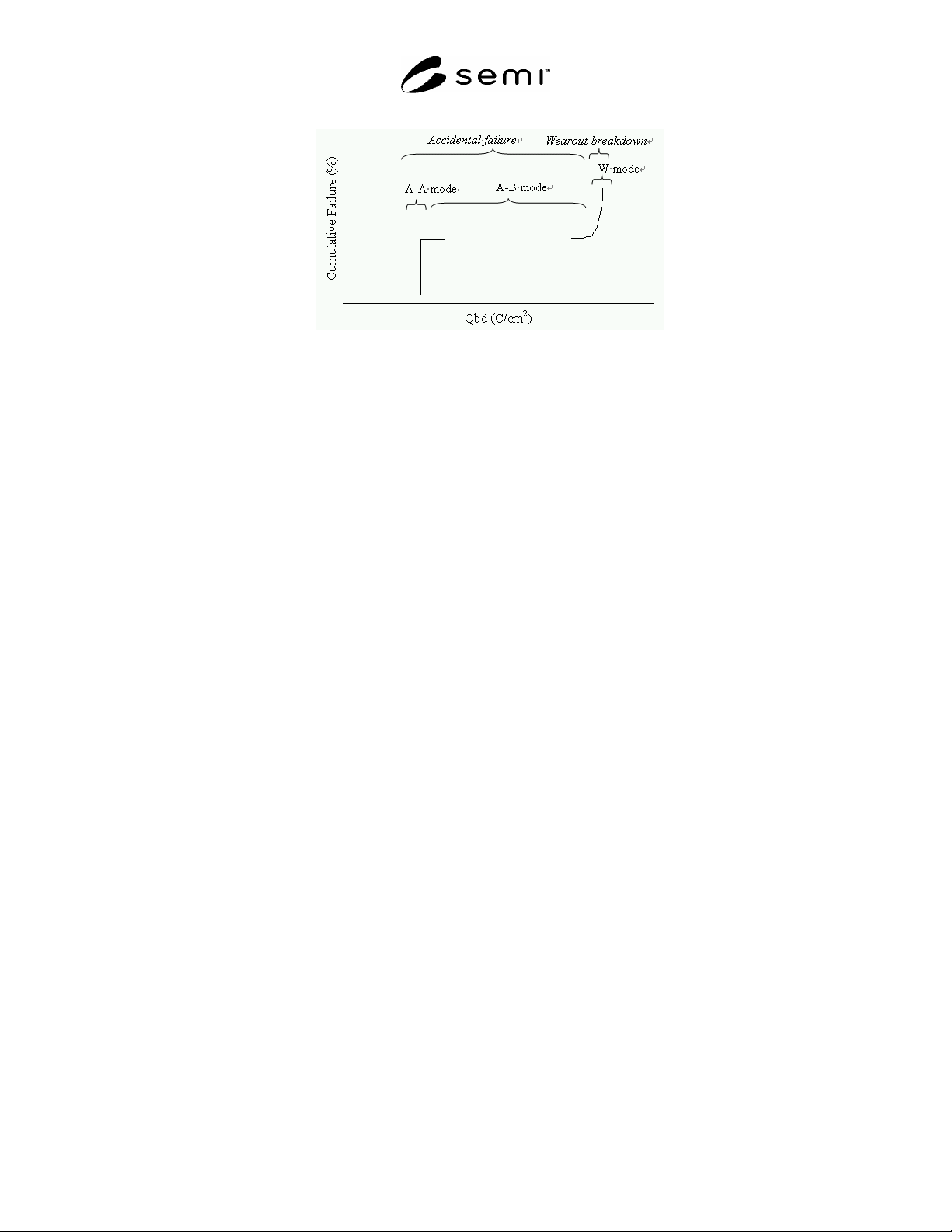
4.2.3.2 Failure Modes — The TDDB Weibull plot
9, 10
is classified to three modes. A typical plot is shown in
Figure 1.
Accidental failure A-A mode
A-B mode
Wearout breakdown W mode
2 Electronic Industries Alliance, EIA Engineering Department, Standards Sales Office, 2001 Eye Street, NW, Washington, D.C. 20006, USA.
Website: www.eia.org
3 Joint Electron Device Engineering Council, 2500 Wilson Blvd., Arlington, VA 22201, website: www.jedec.org
4 J. Ryuta, E. Morita, T. Tanaka and Y. Shimanuki, “Crystal – Originated Singularities on Si Wafer Surface after SC1 Cleaning”, Jpn. J.
Appl. Phys. 29(1990) L947.
5 W. Kern and D. Puotinen, “Clean Solution Based on Hydrogen Peroxide for Use in Silicon Semiconductor Technology”, RCA Rev., 31,
187(1970).
6 T. Mera, J. Jablonski, K. Nagai, and M. Watanabe, “Grown-in defects in silicon crystals responsible for gate oxide integrity deterioration”,
Ohyo-Buturi, 66(7), 728 (1997).
7 K.Yamabe and K.Imai,”Nonplanar Oxidation and Reduction of Oxide Leakage Currents at Silicon Corners by Rounding-off Oxidation”, IEEE
Trans. Electron Devices, ED–34, 1681(1987).
8 K.Yamabe, Y.Shimada, M.Piao, T.Yamazaki, T.Otsuki, R.Takeda, Y.Ohta, S.Jimbo, and M.Watanabe, “Effect of SiO
2
Thickness on Dielectric
Breakdown Defect Density Due to Surface Crystal–Originated Particles”, J.Electrochem.Soc., 150, F42(2003).
9 D. L. Crook, “Method of Determining Reliability Screens for Time Dependent Dielectric Breakdown”, Proc. Int. Reliability Physics
Symposium, 1979, p.1.
10 E. S. Anolick and G. R. Nelson, “Low Field Time Dependent Dielectric Integrity”, Proc. Int. Reliability Physics Symposium, 1978, p.8.
SEMI M60-0305 © SEMI 2005 4
Figure 1
Classification in Weibull plot of TDDB result.
4.2.3.2.1 Discussion on failure modes:
A-A Mode: Initial breakdown failure
o This failure is caused by defects generated during gate oxide formation process such as pinholes and also
by crystal defects such as COPs. This failure corresponds to the A mode and partly B mode failures of
TZDB.
A-B Mode: Intermediate breakdown failure
o This failure is caused by extrinsic defects which are not serious enough to cause the A-A mode. This
failure corresponds to the B mode and partly C mode failure of TZDB.
W Mode: Wearout breakdown
o This breakdown is also called intrinsic breakdown or fatigue breakdown, and relates to the intrinsic lifetime
of oxide films. The measurement of this breakdown shall be performed carefully because the result
depends on measurement conditions.
o Response rapidity of the measurement system has a great influence on A-A mode detection. The total
number of A-A and A-B mode failures is related to the crystal quality of the mirror-polished CZ Si wafers.
4.2.3.3 Categorization of Breakdown Modes — boundaries of A-A/A-B modes and A-B/W modes shall be defined
in advance.
4.2.3.3.1 A-A/A-B Mode Boundary
The detectable minimum Q
bd
values depend on the stress current and response speed of the measurement
systems. As stress current density increases, the charge density of the A-A/A-B mode boundary may also
increases. This effect shall be considered when defining the A-A/A-B mode boundary. Based on these round
robin results, the charge density range from 0.0001C/cm
2
to 0.01 C/cm
2
is recommended as the A-A/A-B mode
boundary.
4.2.3.3.2 A-B/W mode boundary
The A-B/W mode boundary is defined in terms of Weibull plots as shown in Figure RI-3. Ideally, it shall be
determined by the intercept point of two approximation lines in the A-B and W mode ranges. If the boundary
charge density is too low (Q < 1 C/cm
2
), one part of the A-B mode breakdown can be counted as the W mode.
Otherwise, if the boundary charge density is too high (Q > 4 C/cm
2
), one part of the W mode breakdown can be
counted as the A-B mode.
In both cases, we have errors in the classification of the failure mode categories, even if the measurement is
accurately carried out and appropriate Weibull plots are obtained. So, the results of this round robin indicate
that the charge density of 2 C/cm
2
is recommended as the A-B/W mode boundary. To measure the failure rates
at the boundary charge density of the A-B/W modes, all samples are not necessarily broken down. If the
determination procedure of the boundary charge density is clear, the application of a predetermined charge

SEMI M60-0305 © SEMI 2005 5
density will give us the approximate failure rate by the A-B mode breakdown. It is necessary to determine the
classification of failure modes in advance. This is because reliabilities depend on the devices fabricated on the
Si wafer (electrode material, gate oxide thickness, operating voltage, etc.). Refer to an example of mode
classification described in Figure RI-2.
4.2.3.4 Time Zero Dielectric Breakdown (TZDB) — one of the dielectric breakdown characteristic of the gate oxide.
4.2.3.4.1 Discussion — To measure TZDB, oxide leakage current is monitored with an electric field applied to the
MOS capacitor stepwise from 0 to 15MV/cm (for example in the case of a 25 nm-thick oxide, actual applied voltage
would be from 0 to 37.5V). The electrode is negatively biased so that the Si surface is in accumulation and the
electric field is applied effectively. Applied electric field (or voltage) is measured when the oxide leakage current
reaches a predetermined value (judgment current), in other words when the gate oxide breaks down. The influence
of COPs on gate oxide breakdown can be estimated from the distribution of breakdown electric field.
5 Summary of Method
5.1 Overview — This test method consists of two parts. The first one is the fabrication of a number of similar MOS
capacitors on silicon wafers, and the second one is the measurement of the electric charge injected just before the
dielectric breakdown of the MOS capacitors. To measure the injected electric charge, the voltage applied to a MOS
capacitor is controlled so that the current is kept constant. The voltage is monitored throughout the test, and the time
from the beginning to a sudden voltage drop which results from the dielectric breakdown of the silicon dioxide film
is measured. The injected electric charge is the product of the measured time and the gate current density.
5.2 MOS Capacitor Fabrication Process — Many MOS capacitors are formed on the test wafer. The MOS
fabrication process consists of wafer cleaning, thermal oxidation, poly-Si deposition, phosphorous doping, activation
heat treatment, photolithography and etching, in the case of using poly-Si electrodes. The details of the MOS
capacitor fabrication process are shown in SEMI M51. When materials other than poly-silicon are used for
electrodes, the process shall be adjusted to the material used. Although thermally grown 20–25 nm-thick gate oxide
films are recommended in SEMI M51, oxide films as thin as 10 nm can be used depending on the situation.
However, measurement shall be performed carefully for oxide films thinner than 3 nm, because breakdown
judgment becomes difficult under the influence of direct tunneling current. See SEMI C3.6, SEMI C3.54, SEMI
C21, SEMI C27, SEMI C28, SEMI C30, SEMI C35, SEMI C38, SEMI C41, SEMI C44, SEMI C54, SEMI C59.
5.3 Fabrication Environment — It is necessary to fabricate MOS capacitors in a clean room environment of 1000 or
better class in total quality. That is, it needs to be confirmed that the A mode failure rate is 10% or less by TZDB
evaluation. The A mode failure depends not only on the particle of work environment atmosphere but also on the
ultrapure water, fixtures, process apparatus, clean clothes, operation rules etc. Heavily contamination such as
alkaline or heavy metal has an important negative effect on the GOI of the oxide.
5.4 Measurement of Electric Characteristic of MOS Capacitors
5.4.1 The dielectric breakdown defect density of the silicon oxide film is evaluated by constant current TDDB
measurement of the MOS capacitors. The evaluation consists of the measurement of charge injected before the
dielectric breakdown of the MOS capacitors. To measure the injected charge, voltage applied to a MOS capacitor is
controlled so that the current is kept constant. The applied voltage is monitored throughout the test, and the time to
sudden voltage drop which results from dielectric breakdown of the silicon dioxide film is measured. The amount of
the injected charge is the product of the measured time and gate current density. The defect density of the oxide
film is evaluated from the Weibull plot (cumulative failure rate) of the dielectric breakdown data of approximately
100 MOS capacitors.