semi合集-English.pdf - 第5442页
SEMI M60-0305 © SEMI 2005 10 Record Sample ID Determine Test Parameter J, T int ., Tmax , Vbd Probe New Cap. Set t = 0 Measure t, Vt t > T max Vt > V b d Reco rd MOS I D &J Stop & T bd = T max More Cap. on …

SEMI M60-0305 © SEMI 2005 9
10.2.9 Check to see if there are any more MOS capacitors to be measured. If so, repeat from ¶10.2.4 until all MOS
capacitors have been tested. A contact probe for all measuring points eliminates the need for repeat of the
measurement, and proceeds to the next wafer.
10.2.10 Report the results.
10.2.11 Figure 3 shows a flow diagram outlining the procedure for this test method.
10.2.12 For the judgment method of breakdown, not only fixed V
bd
but variation in voltage (V) monitored could
be used.
10.2.13 Figure 4 shows a flow diagram outlining the procedure for the test method when the judgment of
breakdown by drop in voltage (V) is adopted.
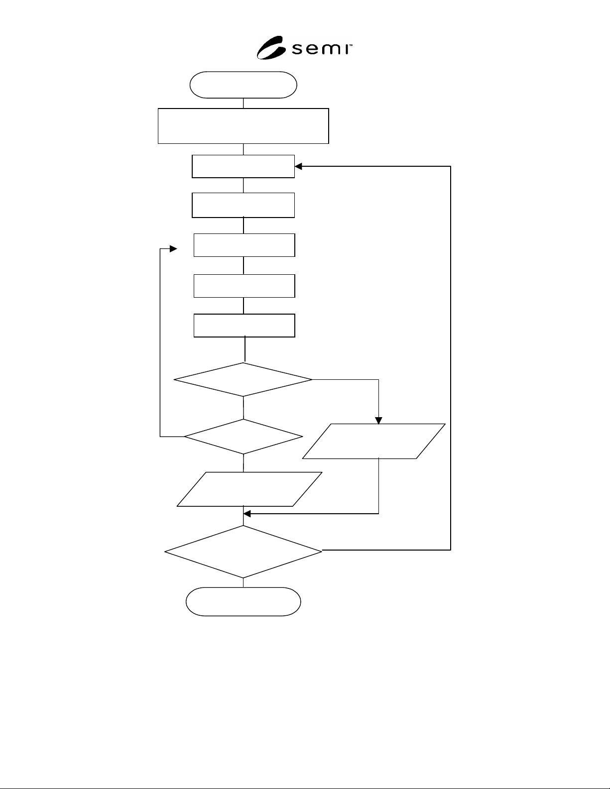
SEMI M60-0305 © SEMI 2005 10
Record Sample ID
Determine Test Parameter
J, T
int
., Tmax, Vbd
Probe New Cap.
Set
t
= 0
Measure t, Vt
t > T
max
Vt > V
b
d
Record MOS ID &J
Stop & T
bd
= T
max
More Cap. on
Wafer?
Report Result
Yes
No
No
Yes
Yes
No
Record MOS ID &
J Stop & T
bd
= Vt
Force J ( I = J/Area)
Wait T
int
.
Figure 3
Flow Diagram Outline (1)
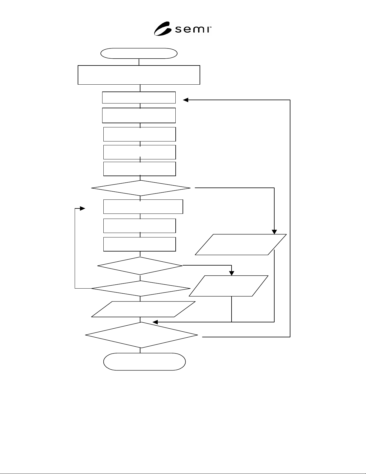
SEMI M60-0305 © SEMI 2005 11
Record Sample ID
Determine Test Parameter
J, T
int
., Tmax,
Δ
V
Probe New Cap.
Set
t
= 0
Measure Vini
Vini
<
Vbd
T > Tmax
Record MOS ID & J
Stop & T
bd
= T
ini
More Cap. on
Wafer?
Report Result
Yes
No
No
Yes
Yes
No
Record MOS ID & J
Stop & T
bd
= Vt
Force J ( I = J/Area)
Wait T
int
.
Measure Vi
Vi
–
Vi-1<
Δ
V
Force J ( I = J/Area)
Wait T
int
.
Record MOS ID
&J stop & T
bd
=
T
max
No
Yes
Figure 4
Flow Diagram Outline (2)