semi合集-English.pdf - 第5492页
SEMI P5-0704 © SEMI 1986, 2004 3 frame wall, and i ts edges m ust be free of visually detectable stringe rs (and particles). Adhesive should form a complete seal between the frame and the m ask over a m inimum of 60% of …
SEMI P5-0704 © SEMI 1986, 2004 2
presence of an AR-coating is determined by agreement
between the user and the supplier.
4.1.2.2 Exposure Range or Wavelength — The
wavelength(s) of the exposure system(s) must be
specified. Table 1 shows the typical exposure
wavelengths.
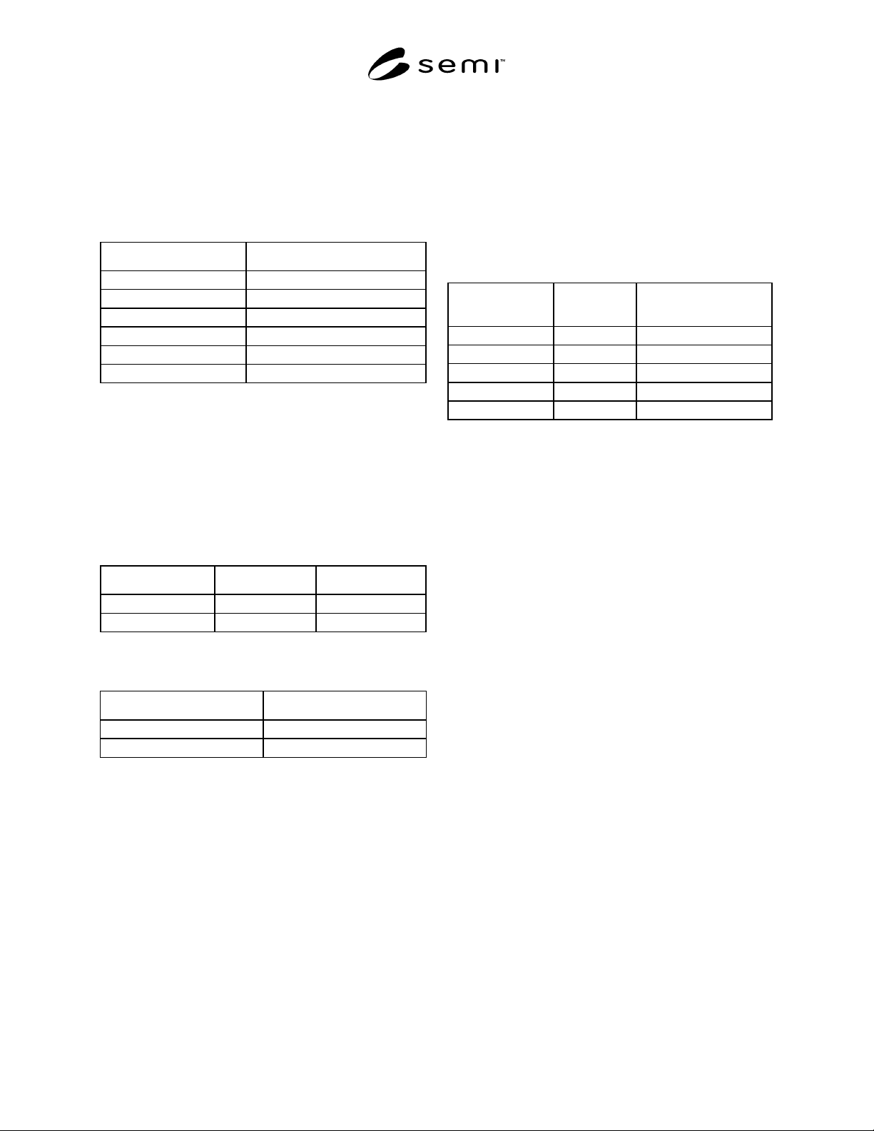
Table 1 Typical Exposure Wavelengths
Terminology Exposure Wavelength(s)
Broadband 360 nm–440 nm
g-line 436 nm
h-line 405 nm
i-line 365 nm
DUV 248 nm
DUV 193 193 nm
4.1.2.3 Optical Transmission — There are two types of
optical transmission depending on the film type. These
are measured at an incident angle of 90° from the
surface of the pellicle at the specified wavelength(s).
The acceptable values are specified in Tables 2 and 3.
The Minimum Transmission given in Table 3 apply to
all wavelengths the film is specified for.
Table 2 Transmission for Broadband Exposure
Systems
Type Average Minimum
AR-Coated ≥ 98 % 96%
Non-AR-Coated ≥ 91 % 82%
Table 3 Transmission for Monochromatic Exposure
Systems
Type Minimum
AR Coated 99%
Non AR Coated 98%
4.1.2.4 Thickness — This is determined by agreement
between user and supplier. The default thickness
tolerance is ± 0.1 µm maximum for Broadband
Exposure Systems and ± 0.05 µm maximum in all other
cases.
4.1.2.5 Mechanical Strength — The pellicle film must
withstand air blow within ranges shown below:
Air pressure: ≤ 2.1 kgf/cm
2
(at input of the air blow
gun).
Nozzle diameter of the air blow gun: ≤ 2 mm.
Distance between the nozzle tip and the film: ≥ 25 mm.
4.1.2.6 Defect Limits — Maximum defect limits are
determined by agreement between the user and the
supplier. These are based on the pellicle standoff, the
numerical aperture and exposure wavelength of the
given type of exposure system, and a typical
specification is given in Table 4. For broadband
exposure systems a typical value of size would be 45
µm, and for monochromatic exposure systems the size
will be significantly smaller.
Table 4 Maximum Defect Limits
Characteristics
Max. No.
Allowable
Size Counted for Max.
No. Allowable
Non-removable
Particles None > size µm
Pinholes None >limit of detection
Scratches None Width > size µm
Dirt None >limit of detection
4.2 In addition, the following items may also be
specified:
4.2.1 Frame Material or Type
4.2.2 Frame Finishing or Coating
4.2.3 Frame Shape, Size and Height
4.2.4 Frame Adhesive Material or Type.
4.2.5 Frame Adhesive Thickness and Width.
4.2.6 Film Adhesive Material or Type
4.2.7 Film Adhesive Thickness and Width.
4.2.8 Film Thickness Uniformity.
4.2.9 Pellicle Vent Mechanism, e.g. vent hole.
4.2.10 Frame inner-wall adhesive.
4.3 If two pellicles will be attached to a photomask
then each pellicle should be independently specified.
For thicker photomask substrates a pellicle is only
attached to the patterned side of the photomask. For
thinner photomask substrates a pellicle is normally
attached to both the patterned and glass sides of the
photomask.
5 Requirements
5.1 Film Adhesive — Film must be sealed on the entire
top of the frame. Seal with a minimum of 50% of the
frame width at any location.
5.2 Frame Adhesive — Frame adhesive must be
continuous and allow no gaps larger than the Defect
Size Limit between pellicle frame and adhesive, and
between adhesive and photomask after attachment. No
part of the frame adhesive may extend beyond the

SEMI P5-0704 © SEMI 1986, 2004 3
frame wall, and its edges must be free of visually
detectable stringers (and particles). Adhesive should
form a complete seal between the frame and the mask
over a minimum of 60% of the width of the frame.
5.3 Frame — Pellicle frame must have no visually
detectable machining burrs, discontinuities in
anodization, or particles.
5.4 Light Resistance
5.4.1 For Broadband Exposure Systems this is
expressed by total exposure energy value (mj/cm
2
or
j/cm
2
) on pellicle film until dropping 1% of optical
transmission of one of the peak wavelengths between
360 nm–440 nm. The test conditions (special
characteristics of exposure wavelength, exposure
energy between 360 nm–440 nm, exposure conditions,
and others) must be stated. Under these conditions, the
pellicle shall release no material, which could
contaminate the photomask or the pellicle itself.
5.4.2 For Monochromatic Exposure Systems this is
expressed by total exposure energy value (mj/cm
2
or
j/cm
2
) of specified wavelength on pellicle’s film until
dropping 0.5% of optical transmission at specified
wavelength. Also, the test conditions (half bandwidth of
exposure specified wavelength, energy of exposure
specified wavelength, exposure conditions, and others)
must be stated. Under these conditions, the pellicle shall
release no material, which could contaminate the
photomask or the pellicle itself.
5.5 Other Characteristics — Other characteristics of
pellicles are to be determined between the supplier and
the user. The transmission of light for mask alignment
is such a characteristic.
6 Measurement Methods
6.1 Measurement methods are to be determined
between the user and supplier. General and example
methods are as follows:
Optical Transmission: by spectrophotometer
Optical Film Thickness: by spectrophotometer
Thickness Uniformity: by monochromatic (e.g., green)
light
Width of Film Adhesive: Visual check by minimum
defect sample
Defects: Visual check by maximum sample or particle
detector
7 Sampling
7.1 Inspection levels shall be agreed upon between the
user and supplier.
8 Handling
8.1 Pellicles are to be handled by the frame only.
9 Certification
9.1 Certification is to be determined between the user
and supplier.
NOTICE: SEMI makes no warranties or
representations as to the suitability of the standards set
forth herein for any particular application. The
determination of the suitability of the standard is solely
the responsibility of the user. Users are cautioned to
refer to manufacturer's instructions, product labels,
product data sheets, and other relevant literature,
respecting any materials or equipment mentioned
herein. These standards are subject to change without
notice.
By publication of this standard, Semiconductor
Equipment and Materials International (SEMI) takes no
position respecting the validity of any patent rights or
copyrights asserted in connection with any items
mentioned in this standard. Users of this standard are
expressly advised that determination of any such patent
rights or copyrights, and the risk of infringement of
such rights are entirely their own responsibility.
Copyright by SEMI® (Semiconductor Equipment and Materials
International), 3081 Zanker Road, San Jose, CA 95134. Reproduction o
f
the contents in whole or in part is forbidden without express written
consent of SEMI.

SEMI P6-88 © SEMI 1988, 19961
SEMI P6-88
SPECIFICATION FOR REGISTRATION MARKS FOR PHOTOMASKS
1 General Specification
1.1 Scope
1.1.1 This specification defines the shape, range of
sizes, and general placement of a registration mark for
use on all photomasks. Methods of use will be stated in
accompanying application notes (to be furnished at a
later date).
1.2 Applicable Documents — None.
2 Detail Specifications
2.1 Introduction
2.1.1 The complete specification for this registration
mark is to be agreed upon by the circuit designer, mask
maker, and the mask user.
2.2 Requirements
2.2.1 This specification covers a defined mark placed
photolithographically on photomasks for the express
purpose of determining the registration accuracy of one
imaged photomask to another imaged photomask within
the same set of photomasks.
2.3 Other
2.3.1 This mark is not intended to be used for the
determination of overlay accuracy of an imaged layer of
a photomask onto a maker to any subsequent imaged
layers on the same wafer.
3 Guidelines for Shape and Sizes of
Registration Mark
3.1 The shape of the mark shall be in the form of a
cross (see Figure 1).
3.2 The area of intersection of the horizontal and
vertical lines shall be “user-defined.” The designer,
mask maker, or user may define any shape of geometry
within this area. The “user-defined” geometry used
shall not exceed the width or height of the area of
intersection (see Figure 2).
3.3 The width of both the horizontal and vertical lines
shall be equal.
3.4 The length of both the horizontal and vertical lines
shall be equal.
3.5 The width and length of the horizontal and vertical
lines may vary due to design rules, scaling, process
bias, etc. Table 1 lists the design dimensions for each
type of photomask. Sections 3.3 and 3.4 are not
superceded by this statement.
3.6 Any of the four quadrants created to the outside of
the cross shall be defined as “No-Man’s Land” and
shall not have any geometry or marks placed within
them (see Figure 3).
3.7 A field or registration mark (i.e., dark or clear) is
user-definable.
3.8 The mark shall be placed as per attached
application notes (to be furnished at a later date).