semi合集-English.pdf - 第5656页
SEMI P10-0705 © SEMI 1990, 2005 151 8.1.810 WAFER_EXPOSURE_SIG MA_OUTER — Outer pa rtial coherence o f the scanner, stepper or ali gner on which the mask is to be used. (This is a unitless parameter.) 8.1.811 WAFER_EXPOS…
SEMI P10-0705 © SEMI 1990, 2005 150
8.1.788 TRANSMISSION_RANGE — For phase shift masks, the maximum acceptable variation of all percent
transmission measurements, relative to each other.
8.1.789 TRANSMISSION_REFERENCE_ONLY — (T or F) If T, indicates that the transmission feature is to be
measured and the data transmitted to the customer (if requested by SHIP_PHASE_SHIFT_MEASUREMENTS), but
that deviations in its measured value due to mask processing would NOT be cause for mask rejection.
8.1.790 TRANSMISSION_TARGET — For phase shift masks, the required percent transmission of light at the
specified PSM_WAVELENGTH compared to quartz.
8.1.791 TRANSMISSION_TOLERANCE — For phase shift masks, the maximum acceptable deviation of the
mean of all percent transmission measurements to the TRANSMISSION_TARGET.
8.1.792 UNSCALED_PATTERN_SIZE — (x,y) Unscaled size of the pattern file. If this is incorrect, the mask will
not be written until it is corrected.
8.1.793 USER_UNIT — To be used for fracturing DATABASE_SOURCE into inspection data, as required by
some inspection systems.
8.1.794 UT1X_UNCUT — (T or F) If T, indicates that the reticle is to be delivered uncut (i.e., 5 inch square) size.
If F, or if the keyword is absent, the reticle is to be delivered in the 3 inch by 5 inch size.
8.1.795 VENDOR — The name of the company from which the masks are ordered.
8.1.796 VENDOR_ADDRESS — Address for VENDOR_CONTACT.
8.1.797 VENDOR_CONTACT — Name of person to contact regarding the mask.
8.1.798 VENDOR_EMAIL — Internet address for VENDOR.
8.1.799 VENDOR_FAX — Phone number for facsimile machine of VENDOR.
8.1.800 VENDOR_ORDER_ID — (text) The mask vendor’s order identification used to track the mask order in
manufacturing.
8.1.801 VENDOR_PHONE — Phone number for VENDOR_CONTACT.
8.1.802 VIRTUAL_ADDRESS — (T or F) Designates whether “virtual addressing” option is to be used to write
the pattern. If T, then the pattern will be written with a writing grid twice the nominal size of the pattern but in such
a way that the overall dimensions of the pattern and its internal features are preserved. This option is used only by
MEBES systems and is usually limited to writing grids no larger than 0.25 micron.
8.1.803 VISUAL_INSP_CRITERIA — (text) The part of the mask to inspect visually (e.g., “5 mm border”).
8.1.804 VISUAL_INSPECTION_OK — (T or F) If T, the area of the preceding pattern may be inspected visually
and/or automatically at the vendor’s option. VISUAL_INSPECTION_OK is not allowed if either
VISUAL_INSPECTION_REQD or AUTO_INSPECTION_REQD is T (true).
8.1.805 VISUAL_INSPECTION_REQD — (T or F) Visual, microscopic inspection of the mask for defects is
required.
8.1.806 WAFER_EXPOSURE_ILLUMINATION — (STANDARD, ANNULAR, DIPOLE, QUADRAPOLE, and
others on request) Illumination configuration of the scanner, stepper or aligner on which the mask is to be used. If
ANNULAR, then both WAFER_EXPOSURE_SIGMA_INNER and WAFER_EXPOSURE_SIGMA_OUTER are
required. If not ANNULAR, then only WAFER_EXPOSURE_SIGMA is required.
8.1.807 WAFER_EXPOSURE_NUMERICAL_APERATURE — Numerical aperture in nanometers of the scanner,
stepper or aligner on which the mask is to be used.
8.1.808 WAFER_EXPOSURE_SIGMA — Partial coherence of the scanner, stepper or aligner on which the mask
is to be used. (This is a unitless parameter.)
8.1.809 WAFER_EXPOSURE_SIGMA_INNER — Inner partial coherence of the scanner, stepper or aligner on
which the mask is to be used. (This is a unitless parameter.)

SEMI P10-0705 © SEMI 1990, 2005 151
8.1.810 WAFER_EXPOSURE_SIGMA_OUTER — Outer partial coherence of the scanner, stepper or aligner on
which the mask is to be used. (This is a unitless parameter.)
8.1.811 WAFER_EXPOSURE_TOOL — Alphanumeric brand and model of the scanner, stepper or aligner on
which the mask is to be used.
8.1.812 WAFER_FAB — (text) Identification of the customer’s wafer fab at which the mask(s) are intended to be
used.
8.1.813 WAIVER — The uniquely identified (for each customer) document which describes specifications which
may be ignored by the vendor.
8.1.814 WAIVER_OVERRIDE — The uniquely identified (for each customer) document which describes
specifications which usually may be ignored by the vendor, but in this case may NOT be ignored by the vendor.
This keyword cancels the effect of the waiver only within the scope of its application in <mask_order>.
8.1.815 WEB_ADDRESS — URL address.
8.1.816 WRITE_DATE_TIME — Date and time at which mask exposure began on the lithography tool.
9 Computing the Checksum
9.1 The cyclic checksum is computed as follows:
9.1.1 Initialize the 16 bit checksum value to zero. Consider all the records in the data file from START_ORDER
through END_ORDER, inclusive. Consider each ASCII character up to and including the “new_line” character.
Convert each character to its ASCII numeric equivalent (e.g., space is 32 decimal, “A” is 65 decimal, etc.) Use the
value 10 decimal for the new_line function regardless of its internal representation (e.g., CR LF). Use only the 7 bit
ASCII representation for each character (i.e., ignore the high order bit in an 8 bit byte).
9.1.2 XOR each of the characters from each of the records in sequence, from the first character in the
START_ORDER record to the new_line character in the END_ORDER record. Before each character is XORed
with the checksum, circularly rotate the previous value of the accumulated 16 bit checksum one bit to the left.
9.1.3 After all of the above characters have been accumulated into the checksum, convert it as an unsigned 16 bit
integer into the ASCII representation of its decimal value. This ASCII string is the data field following the
CHECKSUM keyword, the last record in the mask order structure.
SEMI P10-0705 © SEMI 1990, 2005 152
RELATED INFORMATION 1
CRITICAL DIMENSION KEYWORDS
NOTICE: This related information is not an official part of SEMI P10 and was derived from the North American
Microlithography Committee. This related information was approved for publication by full letter ballot on
April 22, 2004.
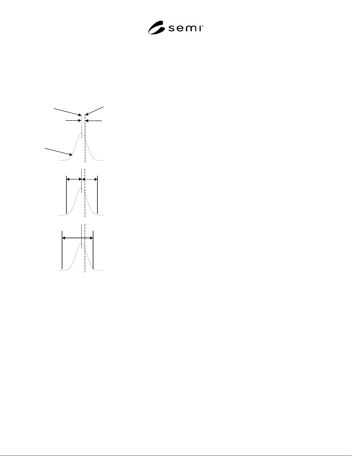
CD_TOLERANCE — Maximum acceptable deviation of the mean of all measured critical
dimensions to the CD_TARGET
CD_RANGE — Maximum acceptable variation of all measured critical dimensions of same
nominal size, same tone and same orientation, relative to each other.
CD_DEVIATION_FROM_MEAN — Maximum acceptable deviation of any of the customer-
required CD measurements from the mean of those measurements.
Mean Target