semi合集-English.pdf - 第5750页
SEMI P19-92 © SEMI 19 92, 1996 1 SEMI P19-92 SPECIFICA TION FOR METROLOGY PATTERN CELLS FOR INTEGRATED CIRCUIT M ANUFACTURE Purpose This docu ment defines several standard test patterns to provide consistent industr ywid…

SEMI P18-92 © SEMI 1992, 2004 2
3.1.9 fraction of good field — the overlay capabilities
of wafer steppers shall be quantified in terms of the
fraction of good fields, F, out of the total number of
fields on the wafer:
F=
N
umber of good fields
N
umber of total fields
Good fields may also be quantified as a percentage
(100 × F%).
3.1.10 Any specification of overlay must define the
applicable exposure field size and the stepping patterns
on the wafers over which the specification applies.
From Sections 3.1.8 and 3.1.9 it follows that the
specification of the overlay capability of wafer steppers
consists of at least two additional numbers, the overlay
value, V, and the fraction of good fields, F. It is
consistent to characterize stepper overlay capability for
multiple overlay values, V
1
, V
2
, ... with corresponding
multiple fractions of good fields, F
1
, F
2
...
NOTICE: SEMI makes no warranties or
representations as to the suitability of the standards set
forth herein for any particular application. The
determination of the suitability of the standard is solely
the responsibility of the user. Users are cautioned to
refer to manufacturer's instructions, product labels,
product data sheets, and other relevant literature,
respecting any materials or equipment mentioned
herein. These standards are subject to change without
notice.
By publication of this standard, Semiconductor
Equipment and Materials International (SEMI) takes no
position respecting the validity of any patent rights or
copyrights asserted in connection with any items
mentioned in this standard. Users of this standard are
expressly advised that determination of any such patent
rights or copyrights, and the risk of infringement of
such rights are entirely their own responsibility.
Copyright by SEMI® (Semiconductor Equipment and Materials
International), 3081 Zanker Road, San Jose, CA 95134. Reproduction of
the contents in whole or in part is forbidden without express written
consent of SEMI.
SEMI P19-92 © SEMI 1992, 19961
SEMI P19-92
SPECIFICATION FOR METROLOGY PATTERN CELLS FOR
INTEGRATED CIRCUIT MANUFACTURE
Purpose
This document defines several standard test patterns to
provide consistent industrywide evaluation and testing
of micropatterning equipment, metrology instruments,
and processes used in integrated circuit manufacturing.
1 General Specification
1.1 Scope
1.1.1 This specification defines the s hape, general
size, and recommended placement and design rules
(where appropriate) of several basic pattern cells for
linewidth metrology, resolution testing, and proximity
testing. These standard patterns include cells that can be
used for optical microscopy, electron microscopy, and
electrical probe testing.
1.1.2 This document does not attempt to specify the
measurement techniques to be used in verifying critical
dimensions for these test patterns on the reticle.
Similarly, this document does not attempt to specify
how the printed patterns are to be measured on the
wafer. This document specifies only what the patterns
are supposed to be; it is left to the user to ensure that
the actual pattern conforms to this specification, subject
to all other applicable SEMI specifications. A separate
SEMI document will specify CD measurement
conditions (see Section 1.2.1).
1.2 Applicable Documents
1.2.1 SEMI Standards
SEMI P24 — CD Metrology Procedures
1.3 Definitions
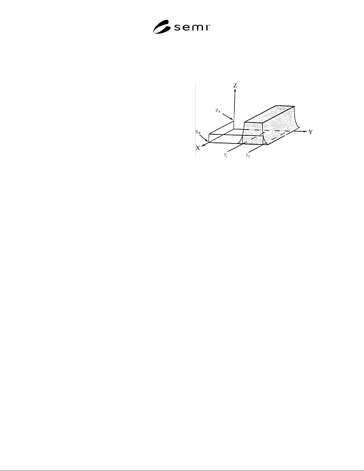
linewidth — In semiconductor technology, at a given
cross-section of the line, the distance between the
airline material boundaries at some specified height
above the interface between the patterned layer in
which the line is formed and the underlying layer (see
Figure 1).
Figure 1
Linewidth (X
0
, Z
0
) = Y
2
- Y
1
NOTE: The physical basis for various methods of measuring
linewidth may result in the measurements being carried out at
differing heights for the same line at the same cross-section.
For this reason, substantial method-dependent differences in
measurement results may be expected and it is convenient to
identify the method used in expressions such as “SEM
linewidth,” “optical linewidth,” or “electrical linewidth”
(ASTM F 127). Furthermore, the height at which the
measurement is taken shall be qualitatively stated, even if it
cannot be quantitively determined.
feature — areas within a single, continuous boundary
(for example, an aggregate image) that have an optical-
density value (gray-level range), that is distinct from
the background area outside the feature (ASTM D
3849, D 24) (e.g., the simplest element of a pattern,
such as a single line, space, or L-bar).
feature group — a small assembly of one or more
similar features arranged together, such as three nested
L-bars.
nominal feature dimension — the linear dimension of
interest, such as the linewidth or contact hole width.
basic cell — an arrangement of features or groups, as
defined by this document, based upon a specific,
nominal-feature dimension.
composite cell — an arrangement of several basic cells.
SEMI P19-92 © SEMI 1992, 1996 2
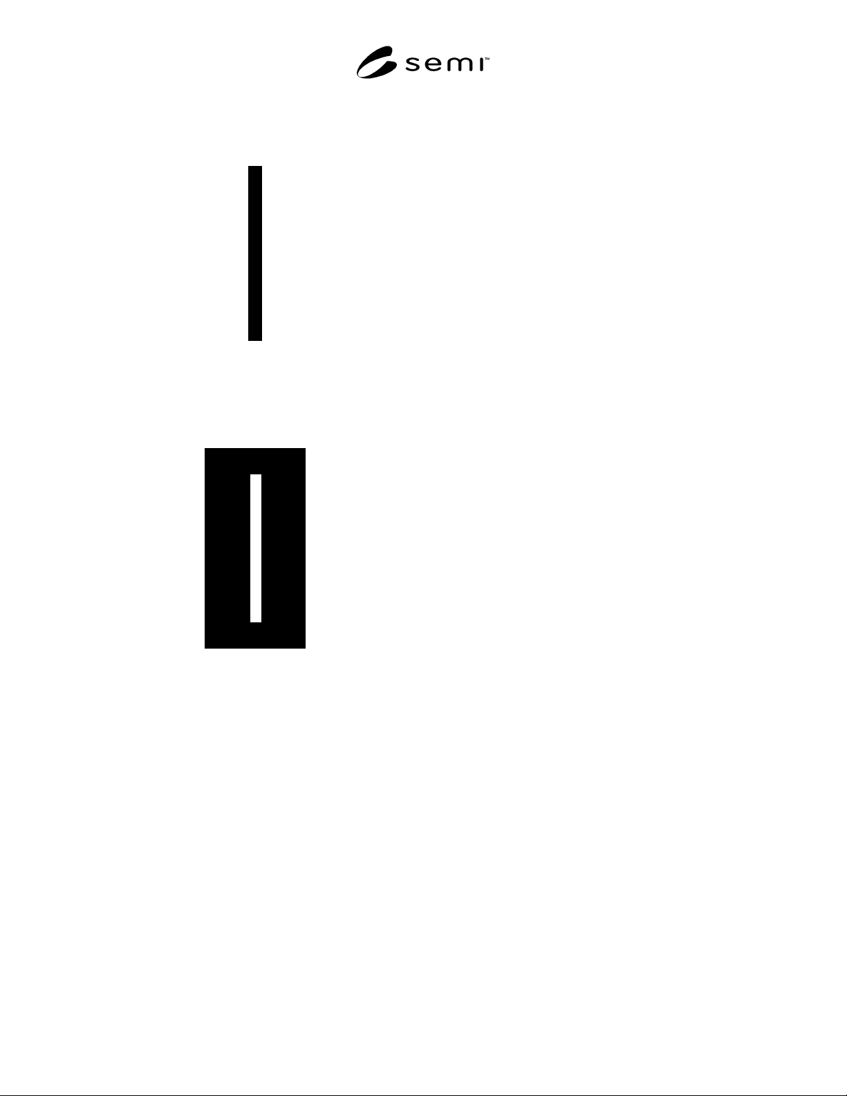
isolated line — a clearfield, dark line as shown in
Figure 2 (SYN: island).
Figure 2
Isolated Line
isolated space — A darkfield, clear line as shown in
Figure 3 (SYN: window, trench, contact, opening).
Figure 3
Isolated Space
2 Detail Specification
2.1 Introduction
2.1.1 This specification describes th e pattern cells,
which are illustrated in the figures at the end of this
document. These cells are to be placed
photolithographically or by other direct patterning
methods onto wafer substrates at different masking
levels during the IC manufacturing process.
2.1.2 Many details of the pattern cel ls, such as the
orientation, magnitude, range of the linewidths, and
polarity of tone (clearfield vs. darkfield) will be defined
by the user, unless otherwise noted. When reporting
results based on tests using these cells, details such as
field polarity, orientation, and topographic
considerations must be indicated.
2.1.3 All critical dimensions given i n this document
are the actual CAD values at 1X. For a given
magnification, M, the target dimensions on the reticle
should be exactly M times the dimension given in this
specification. The reticle dimensions must not be sized
to compensate for any wafer process-induced bias.
2.2 Applications
2.2.1 These cells are intended to be used in several
applications. The following applications list some of the
intended uses for the pattern cells.
2.2.1.1 in-line process monitoring — To establish
patterns to determine if the layer has been processed to
design specifications.
2.2.1.2 process transfer — To standardize the patterns
for process monitoring within manufacturing
fabrication sites and to facilitate process and technology
transfers between sites.
2.2.1.3 equipment evaluation — To standardize the
patterns used to evaluate semiconductor equipment.
2.2.1.4 equipment characterization — To standardize
the patterns for the characterization process of different
metrology equipment.
3 Guidelines for Application s
3.1 General
3.1.1 The cells described here repres ent a primary
metrology set from which composite patterns may be
constructed.
3.1.2 A composite pattern set meets this standard if it
consists of any number of the basic cells described
herein, provided all design rules for each cell are
obeyed.
3.1.3 Each basic cell contains a fundamental design
feature. This feature may be repeated at different (user-
defined) dimensions within a modified metrology cell.
The user will determine all appropriate dimensions for
the feature as they apply to specific
processing/equipment situations.
3.1.4 The figures provided within th is document are
intended to illustrate the proper layout of each pattern
cell and to define the appropriate design elements used
within each basic cell. The pattern cell dimensions are
provided when appropriate.
3.1.5 All feature groups must be separated by at least
five times the largest feature width. This proximity rule
is defined in order to ensure that patterns intended to be
independent are indeed non-coupled.