semi合集-English.pdf - 第5763页
SEMI P20-0703 © SEMI 1992, 2003 2 7.1.2 Conditions — Specify condi tions described in Sections 5.2.1 to 5.2.4. 8 Exposure 8.1 Defines exposure condition description methods for resist param eter descriptions in and after…

SEMI P20-0703 © SEMI 1992, 2003 1
SEMI P20-0703
GUIDELINE FOR CATALOG PUBLICATION OF EB RESIST
PARAMETERS (PROPOSAL)
This guideline was technically approved by the Global Micropatterning Committee and is the direct
responsibility of the Japanese Micropatterning Committee. Current edition approved by the Japanese
Regional Standards Committee on April 28, 2003. Initially available at www.semi.org June 2003; to be
published July 2003. Originally published in 1992.
1 Purpose
1.1 The purpose of this guideline is to provide a
baseline for publications of EB resist parameters. It can
also be used as a guide to evaluate resist process
parameters. This guideline is intended to be applicable
for electron beam processes.
1.2 The parameters for EB Resist publication are
discussed below.
2 Scope
NOTICE: This standard does not purport to address
safety issues, if any, associated with its use. It is the
responsibility of the users of this standard to establish
appropriate safety and health practices and determine
the applicability of regulatory or other limitations prior
to use.
3 Resist Commercial Name
3.1 Describe resist commercial name.
4 Resist Properties
4.1 Polymer Properties
4.1.1 Components — Describe resist components.
Chemical structure is not necessarily required.
4.1.2 Molecular Weight — Describe M
w
, Mn and
M
w
/Mn if known.
4.1.3 Thermal Characteristics — Describe Tg and Tm.
4.2 Resist Solution Properties
4.2.1 Solvent — Specify chemical names.
4.2.2 Viscosity — Solution viscosity, mPa·s, 25°C.
4.2.3 Solid Content — Weight %.
5 Film Forming Properties
5.1 Thickness Curves — Plot film thickness T (µm or
nm) after prebake versus spinning speed R (rpm). Here,
x axis is log (R) and y axis is log (T).
5.2 Conditions — Specify following conditions.
5.2.1 Substrate — Silicon wafer or chrome mask
blank. Specify its structure.
5.2.2 Spinning Conditions — Specify spinning
conditions including coating sequence.
5.2.3 Environmental Conditions — Temperature (°C),
relative humidity (%).
5.2.4 Prebake Conditions — Prebaking temperature
(°C), time (sec), heating and cooling method and
apparatus. Specify heating rate and cooling rate if
monitored.
5.2.5 Thickness Measurement Methods — Thickness
measurement instruments and measurement method. In
case of a light interferance thickness measurement
apparatus, specify the refractive index as a parameter
used in the measurement.
6 Film Thicknesses
6.1 Defines resist thicknesses and measurement
conditions for resist parameter descriptions in and after
Section 10. Unit is µm or nm.
6.1.1 Film Thickness Definitions
6.1.1.1 Ti — Initial thickness after prebake prior to
exposure.
6.1.1.2 Te — Exposed region thickness after
development.
6.1.1.3 Tu — Unexposed region thickness after
development, and after postbake if required.
6.1.1.4 NTe — Te/Ti. Normalized exposed region
thickness.
6.1.1.5 NTu — Tu/Ti. Normalized unexposed region
thickness.
6.1.2 Thickness Measurement Conditions — Thickness
measurement conditions should be the same as
described in Section 5.2.5. In case of measurements of
exposed region thickness, exposed region area should
be larger than 20 µm on all sides.
7 Sample Preparation
7.1 Defines sample preparation methods for resist
parameter descriptions in and after Section 10.
7.1.1 Film Thickness — Ti. 0.50 ± 0.02 µm (500 ± 20
nm) is recommended for a standard thickness.

SEMI P20-0703 © SEMI 1992, 2003 2
7.1.2 Conditions — Specify conditions described in
Sections 5.2.1 to 5.2.4.
8 Exposure
8.1 Defines exposure condition description methods for
resist parameter descriptions in and after Section 10.
8.1.1 Exposure Dosage Definition — Quantity of
electrical charge per unit area, µC/cm
2
. Describe as D.
8.1.2 Exposure Dosage Calculation — Calculate as
follows.
D = I × t/S × 10
6
Here, I is current (A), t is exposure time (s), S is
exposure area (cm
2
).
Specify these parameters.
8.1.3 Acceleration Voltage — In a range from 10 to 50
kV.
8.1.4 Exposure System — Specify exposure methods.
8.1.4.1 Beam Scanning Methods — For example, raster
scanning or vector scanning. Specify beam scanning
pitch if defined.
8.1.4.2 Beam Shape — Describe beam shape.
8.1.4.3 Beam Conditions — Specify beam size (µm or
nm) and current density (A/cm
2
), if possible.
8.1.4.4 Exposure Tool Manufacturer and System Name
— Specify exposure tool manufacturer and system
name, if possible.
9 Processing and Developing Parameters
9.1 This section defines process condition descriptions
in and after Section 10.
9.1.1 Post Exposure Treatments — Describe if any
treatment is processed after exposure before
development.
9.1.1.1 Methods — For example, post exposure bake.
9.1.1.2 Conditions — For example, treatment
conditions such as temperature (°C), time (s),
atmosphere, heating method, cooling method and
apparatus. Specify heating rate and cooling rate if
monitored.
9.1.2 Developing Parameters
9.1.2.1 Methods — Specify spray, dip, or puddle.
9.1.2.2 Solution Components — Specify name of
developer and rinse. (Chemical names and weight
percent if possible.)
9.1.2.3 Temperature — °C
• For spray, bulk temperature. Processing chamber
atmospheric temperature if monitored.
• For dip, solution temperature.
• For puddle, bulk temperature. Processing chamber
atmospheric temperature and substrate temperature
if monitored.
9.1.2.4 Time — sec.
9.1.2.5 Relative Humidity — %.
9.1.2.6 Additional Processes — Specify if applied.
9.1.3 Post bake
9.1.3.1 Conditions — Temperature (°C), time (s),
heating method, cooling method, and apparatus.
Specify heating rate and cooling rate if monitored.
9.1.3.2 Describe treatment conditions before or after
post baking, if applied.
10 Sensitivity Curves
10.1 Curve Plotting — Plot NTe as a function of D.
Here, x axis is log (D), y axis is NTe.
10.2 Exposure Dosage Range
10.2.1 Positive Resist — Include dosages larger than a
dose gives NTe of 0.
10.2.2 Negative Resist — Include dosages larger than a
dose gives NTe of 0.7.
11 Sensitivity
11.1 A dose required to form a pattern larger than 20
µm on all sides.
11.1.1 Positive Resist — Describe as Dp
0
. It gives NTe
of 0.
11.1.2 Negative Resist — Describe as Dn
0.5
. It gives
NTe of 0.5.
12 Contrast
12.1 Contrast Definition — Describe as γ. Calculate
from a slope of resist sensitivity curve.
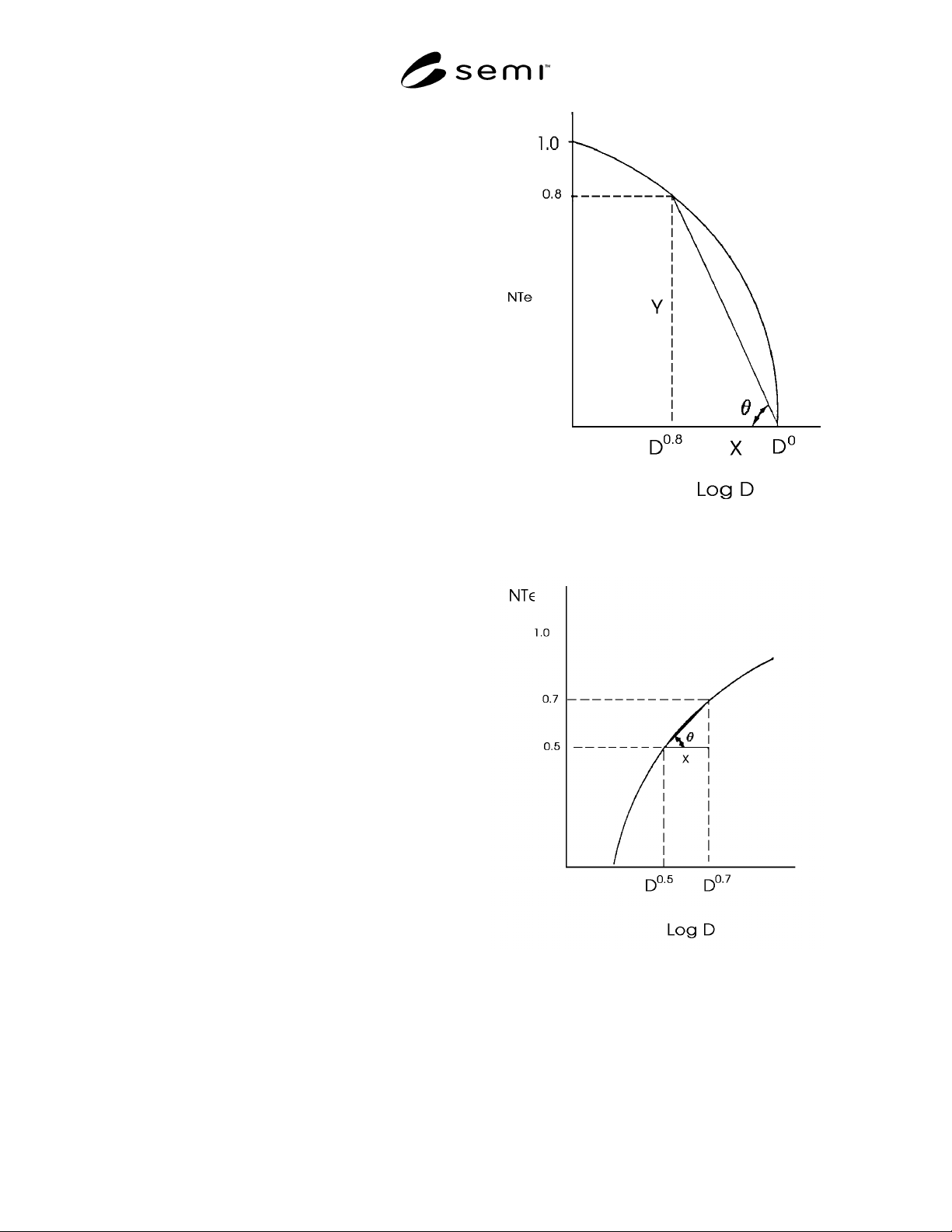
12.2 Positive Resist (Figure 1) — Calculate using an
angle given from a solid line between NTe of 0 and
NTe of 0.8 and a solid line parallel to x axis. Here, NTu
should be larger than 0.9.
γ
p
0
−
0.8
=
tan
θ
=
y/x
=
0.8/log (Dp
0
/Dp
0.8
)
SEMI P20-0703 © SEMI 1992, 2003 3
12.3 Negative Resist (Figure 2) — Calculate using an
angle given from a solid line between NTe of 0.5 and
NTe of 0.7 and a solid line parallel to x axis.
γ
p
0.5
−
0.7
= tanθ = y/x = 0.2/log (Dn
0.7
/Dn
0.5
)
13 Resolution
13.1 Pattern Type and Feature Size — Lines and
spaces. Ratio of lines and spaces should be 1:1. Add
hole pattern and isolated pattern if possible.
13.2 Conditions — Specify conditions in Sections 7, 8,
and 9.
13.3 Measurement Method — Measure resolutions
using a scanning electron microscope.
14 Nominal Exposure Dosage
14.1 Nominal Exposure Dosage Definition — A dose
which gives lines and spaces of 3 µm at a ratio of 1:1
under conditions described in Sections 7, 8, and 9.
15 Others
15.1 Describe following items if known.
15.1.1 Durability — Wet etching, dry etching.
15.1.2 Stability — Shelf stability, spun film stability,
post exposure stability, and post processing stability.
15.1.3 Removability — Describe resist removing
method after processing.
15.1.4 Remarks — Describe special characteristics of
the EB resist.
15.1.5 Cautions — Describe cautions for safety.
(Reference) G.N. Taylor, Solid State Technology, June
(1984) 105.
Figure 1
Positive Sensitivity Curve
Figure 2
Negative Sensitivity Curve