semi合集-English.pdf - 第5819页
SEMI P25-94 © SEMI 1994, 2004 5 b. Alternatively, if point- like objects are available in the image for evaluation, the focal surface may be obtained by findi ng the z displacement for the best processed point image at e…

SEMI P25-94 © SEMI 1994, 2004 4
permissible deviations. The depth of focus maps may be
dependant, among other things, on the process, line width,
and image geometry, especially the choice of point-like
patterns or line-like patterns along the saggital, tangential, or
other directions. Several maps may be produced as part of a
test, covering these variations.
6 Procedure
6.1 Pattern — See SEMI P19. A pattern and pattern
dimensions are to be selected in accordance with the
most reasonable correspondence to the intended
application of the equipment. Typically, the pattern will
consist of two sets of evaluative lines. A sequence of
patterns of varying line widths may also be employed,
in which case the depth of focus may be reported as a
function of the line width. The pattern selection and
dimensions must be included as part of the report.
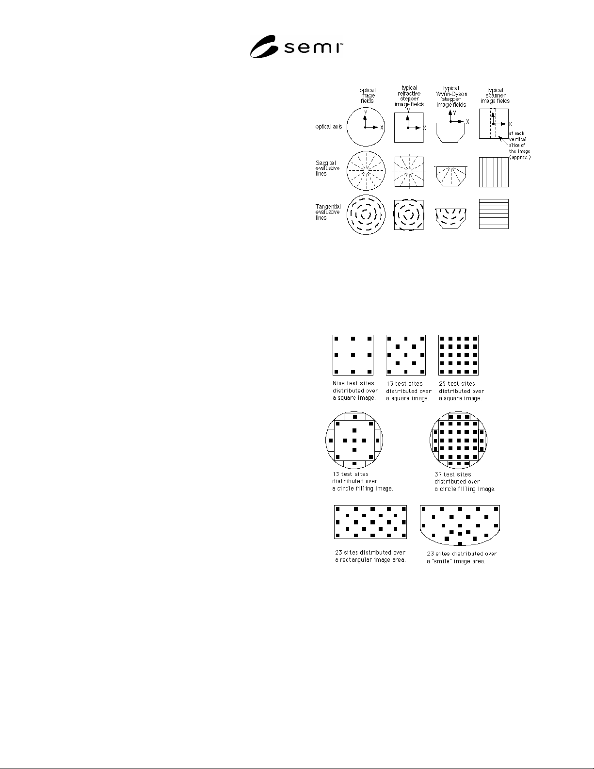
6.2 Test Sites — The pattern is to be repeated at least
nine times over the image field. The minimum of nine
sites will include the four corners of the image, the four
edge midpoints of the image field and the center of the
image field. Whichever many sites are used, the sites
must be distributed symmetrical and uniformly over the
image field, giving no special weight to any portion of
the image field. For examples, see Figure 2.
6.3 Process — A test image will be printed under the
same conditions and processes to be used in the
practical application (see Section 2) of the instrument
(stepper, scanner, etc.). The process description will be
included in the depth of focus and best focus report.
6.4 Focus Steps — The image will be printed several
times, varying the defocus by a fixed amount between
each print. The amount of variation of defocus between
steps and the limits of the defocus will be selected so as
to bracket the expected best focus position and to reach
beyond the depth of focus at the extremes of the image
series, as best as can be determined. The number and
size of the defocus steps must be specified in the report.
6.5 Image Array — These multiple images can be a
row of separate exposure fields on one substrate,
multiple stepped displaced exposures of the test
geometry within one image field region, or even
exposures on entirely separate substrates. The particular
strategy is usually constrained by the functions of the
instrument under test.
6.6 Test Measurements — For each image site for both
test pattern orientations and at each value of defocus,
the processed image geometries will be examined and
either accepted or rejected on the basis of image
sharpness, image size or some related image
characteristic. Usually this examination will use the line
width as the acceptance criteria. The total number of the
measurements will be twice the number of sites times
the number of defocus steps.
6.7 Quantitative Image Evaluation — The photoresist
image patterns will be examined or measured for
deviation from the target, in a manner specified by the
vendor or user of the instrument. An acceptable image
is where the variation of the pattern is not outside the
permissible deviation under the conditions of the
intended use of the equipment. The defocus values for
which the image is usable will be determined at each
image site within the image field.
6.8 Depth of Focus and Best Focus Determination —
The defocus variation over which there are usable
images at simultaneously every test site within the field,
by the above criteria, will be reported as the practical
focal range. In accordance with the definition, the best
focus will be the z axis position where some target
specification is met or the possible defocus is
maximized or the line deviation minimized, etc. If there
is no common range of usable defocus across the field,
the depth of focus is zero and the best focus is
undetermined. This can occur due to, among other
things, a large plane tilt of substrate to the optical axis,
high aerial image focus surface curvature, high
astigmatism, and auto focus system instabilities.
6.9 Focal Astigmatism Determination — The test
measurements are separated into two groups, one group
for each of the two different orthogonal orientations of
the test pattern. These groups are referred to as the “S”
and “T” groups, however the saggital and tangential
orientations have not necessarily been used in
accordance with the definition of “rotated astigmatism.”
6.9.1 For each group separately, the focal surface is
determined by using for each site the midpoint of the
defocus values where the processed image is found to
be acceptable, in accordance with Section 6.7.
6.9.2 The difference in z position between these
surfaces for each image site is calculated. These
differences are plotted as a function of image position.
This map of values is the astigmatism.
6.9.3 The maximum of the absolute values is the
maximum astigmatism.
6.9.4 The average of the absolute values is the mean
astigmatism.
6.10 Field Flatness Determination — Two alternative
but essentially equivalent methods of determining the
focal surface are allowed:
a. The focal surface which is the midpoint of the S and
T focal surfaces is calculated.
SEMI P25-94 © SEMI 1994, 2004 5
b. Alternatively, if point-like objects are available in
the image for evaluation, the focal surface may be
obtained by finding the z displacement for the best
processed point image at each image site.
6.10.1 This focal surface is reported as a map of z
displacements as a function of image position. This
map is the curvature of field.
6.10.2 The difference between the minimum z
displacement in the focal surface and the maximum z
displacement in the focal surface is the maximum
curvature of field.
NOTE 21: This includes optical image curvature, wafer
curvature, fixture curvature, etc. This procedure for the sake
of simplicity does not separate these effects. It is an error to
consider this measure of field flatness equivalent to a measure
of the optical image focal surface.
7 Report
7.1 The depth of focus, best focus, etc. reports will
include a description of the practical use, per definition
5.1.5. In addition, the report should include mention of
any special mechanical considerations — in particular,
among others, mention should be made if a chip
leveling scheme is used and whether this scheme is site
by site or global.
7.2 List of report contents:
Process: substrate and layer types and processing,
exposure conditions
Pattern: description or diagram of the test
structures, including the choice of S and T or X and
Y orientations
Wafer: the wafer quality and specifications.
Leveling: leveling mechanism.
Sites: list or map of the image sites.
Criteria: the acceptance criteria used in the
evaluation of the test structures.
Depth of Focus or Focal Range (single overall
values)
Best Focus (single overall value)
Astigmatism map
Maximum Astigmatism
Mean Astigmatism
Field Flatness map
Maximum Curvature of Field
Figure 1
The Coordinate System and the Sagittal and
Tangential Lines, Shown for the Optical Image
Cylindrical Symmetry and for the Actual
Processed Images of Steppers and Scanners
Figure 2
Typical Test Site Placements in
Various Types of Image Fields

SEMI P25-94 © SEMI 1994, 2004 6
NOTICE: SEMI makes no warranties or representations as to the suitability of the standards set forth herein for any
particular application. The determination of the suitability of the standard is solely the responsibility of the user.
Users are cautioned to refer to manufacturer's instructions, product labels, product data sheets, and other relevant
literature, respecting any materials or equipment mentioned herein. These standards are subject to change without
notice.
By publication of this standard, Semiconductor Equipment and Materials International (SEMI) takes no position
respecting the validity of any patent rights or copyrights asserted in connection with any items mentioned in this
standard. Users of this standard are expressly advised that determination of any such patent rights or copyrights, and
the risk of infringement of such rights are entirely their own responsibility.
Copyright by SEMI® (Semiconductor Equipment and Materials
International), 3081 Zanker Road, San Jose, CA 95134. Reproduction of
the contents in whole or in part is forbidden without express written
consent of SEMI.