semi合集-English.pdf - 第5849页
SEMI P33-0998 © SEMI 1998 3 Table 1 Specific ations for Edge Length, Squar eness, and Thickness for Sq uare Substrates Nominal E dge Length Edge Le ngth Minimu m Edge Le ngth Maximum Sq uareness Thickn ess Minimu m Thick…

SEMI P33-0998 © SEMI 1998 2
near future. Flatness of 0.5 µm is very desirable for
semiconductor production, and equipment suppliers
may want to consider this in their designs.)
9 Visual Criteria
9.1 A visual quality area, which may or may not
correspond with the flatness area, shall be agreed upon
between the user and supplier.
9.2 Fused silica (ULTE) substrates shall be identified
with one corner chamfer as shown in Figure 5.
Dimensions of the chamfer shall be as specified in
Figure 6. The corner chamfer is made only on the non-
critical side of the substrate.
10 Sampling
10.1 Unless otherwise specified, appropriate sample
sizes shall be selected from each lot in accordance with
ANSI/ASQC Z1.4. Each quality characteristic shall be
assigned an acceptable quality level (AQL) in
accordance with ANSI/ASQC Z1.4 definitions for
critical, major, and minor classifications. If desired,
and so specified in the contract or order, each of these
classifications may alternatively be assigned cumulative
AQL values. Inspection levels shall be agreed upon
between user and supplier.
11 Test Methods
11.1 Thermal Expansion — Determine in accordance
with ASTM E 228.
11.2 Flatness (to be agreed upon between user and
supplier).
11.3 Visual (to be agreed upon between user and
supplier).
11.4 Parallelism (to be agreed upon between user and
supplier; non-contact methods are preferred).
12 Handling
12.1 Substrates are to be handled on the edges only.
Substrates are to be handled with gloves approved for
cleanroom use, when human handling is required.
13 Orientation
13.1 For ULTE substrates with a single corner
chamfer (see Section 9.2), it is recommended that all
orientation be performed referencing the corner of the
substrate diagonally opposite the chamfer. See Figure 8
for more information.
14 Certification
14.1 Upon request of the purchaser in the contract or
order, a manufacturer’s or supplier’s certification that
the material was manufactured and tested in accordance
with this specification, together with a report of the test
results, shall be furnished at the time of shipment.
15 Packing and Marking
15.1 Substrates shall be packed in a class 100
environment as defined by Federal Standard 209.
Containers shall be designed to prevent glass-to-glass
contact, and to protect the substrates from
contamination in handling and transit. Substrates shall
be shipped with the critical side toward the front or
bottom of the shipping carrier, depending on carrier
configuration. The substrate shipping position shall be
indicated on each container. Packaging shall comply
with the applicable internal, national, state, and local
laws and regulations required for shipping.
15.2 Containers shall be labeled “Warning: Open and
Handle Under Cleanroom Conditions Only” as well as
identified by user purchase order number (if
applicable), drawing number (if applicable), quantity,
supplier lot number, and material identification.
16 Related Documents
16.1 SEMI Standard
SEMI P1 — Specification for Hard Surface Photomask
Substrates
SEMI P33-0998 © SEMI 19983
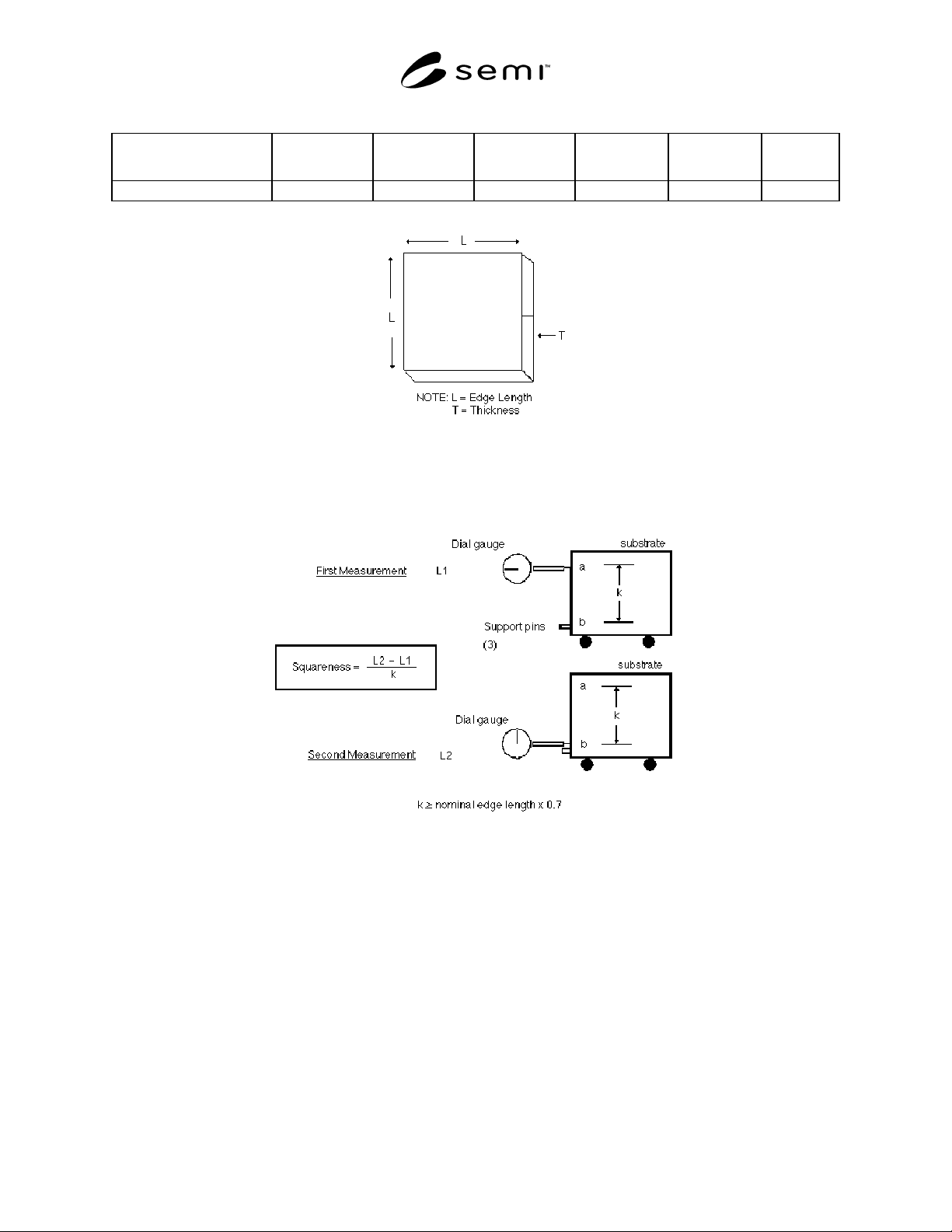
Table 1 Specifications for Edge Length, Squareness, and Thickness for Square Substrates
Nominal Edge Length
Edge Length
Minimum
Edge Length
Maximum Squareness
Thickness
Minimum
Thickness
Maximum Units
230 mm 229.6 230.0 0.186/213 8.90 9.10 mm
Figure 1
Square Hard Surface Photomask Substrate
Figure 2
Measurement Fixture and Calculation to Determine Substrate Squareness
SEMI P33-0998 © SEMI 1998 4
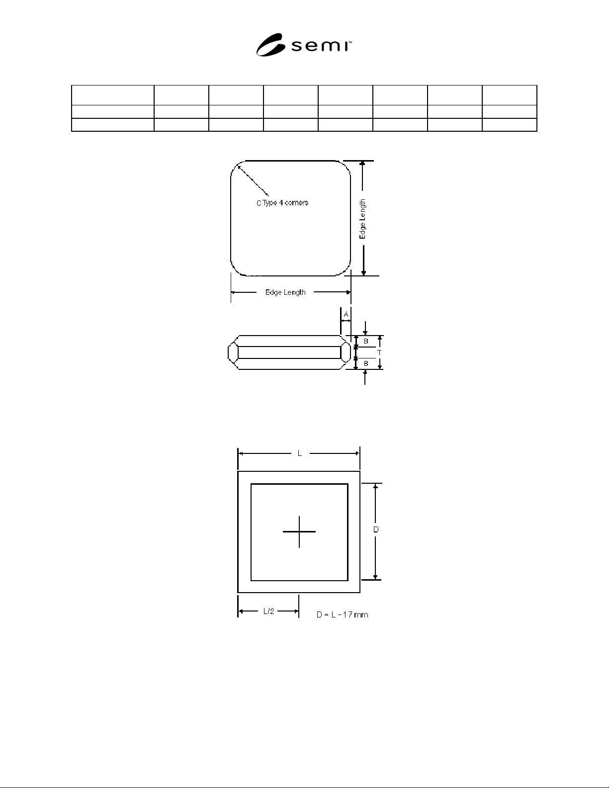
Table 2 Specifications for Beveled and Rounded Edge Dimensions
T AABBCC
Nominal Minimum Maximum Minimum Maximum Minimum Maximum Units
9.00 0.20 0.60 0.20 0.60 2.00 3.00 mm
NOTE: “D” is radius of curvature of concerns.
Figure 3
Beveled Edge Dimensions
Figure 4
Square Quality Area