semi合集-English.pdf - 第5853页
SEMI P33-0998 © SEMI 1998 7 A P PENDIX 1 HARD SURFACE PHOTOMASK MA TERI A L PROPERTIES NOT E: This a ppendix w as approve d as a n off icial part of SEMI P33 by full letter-ballot procedure. Table A1-1 Material Propertie…
SEMI P33-0998 © SEMI 1998 6
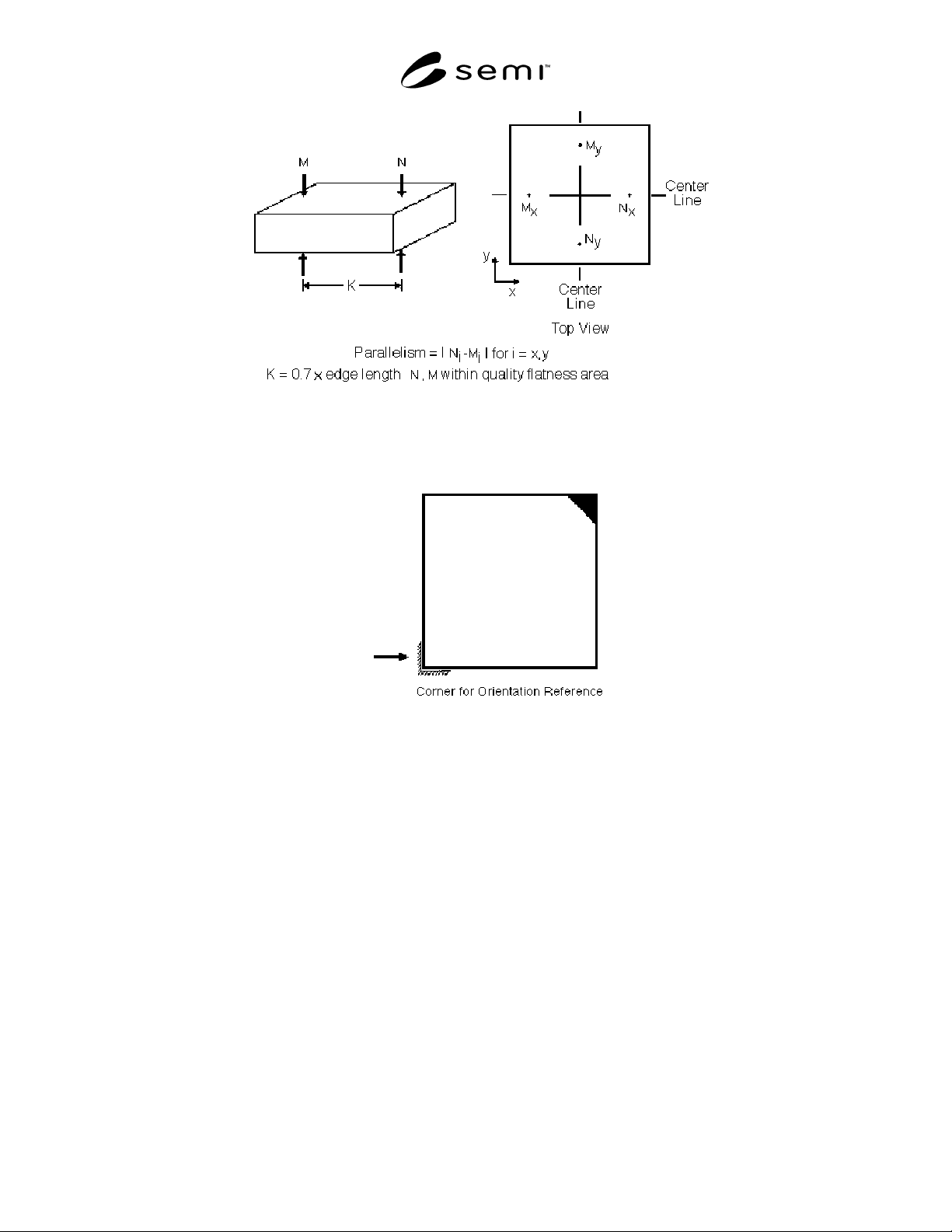
Figure 7
Measurements for Calculation of Parallelism with Approximate Positions
Figure 8
Corner Diagonally Opposite of Chamfer
SEMI P33-0998 © SEMI 19987
APPENDIX 1
HARD SURFACE PHOTOMASK MATERIAL PROPERTIES
NOTE: This appendix was approved as an official part of SEMI P33 by full letter-ballot procedure.
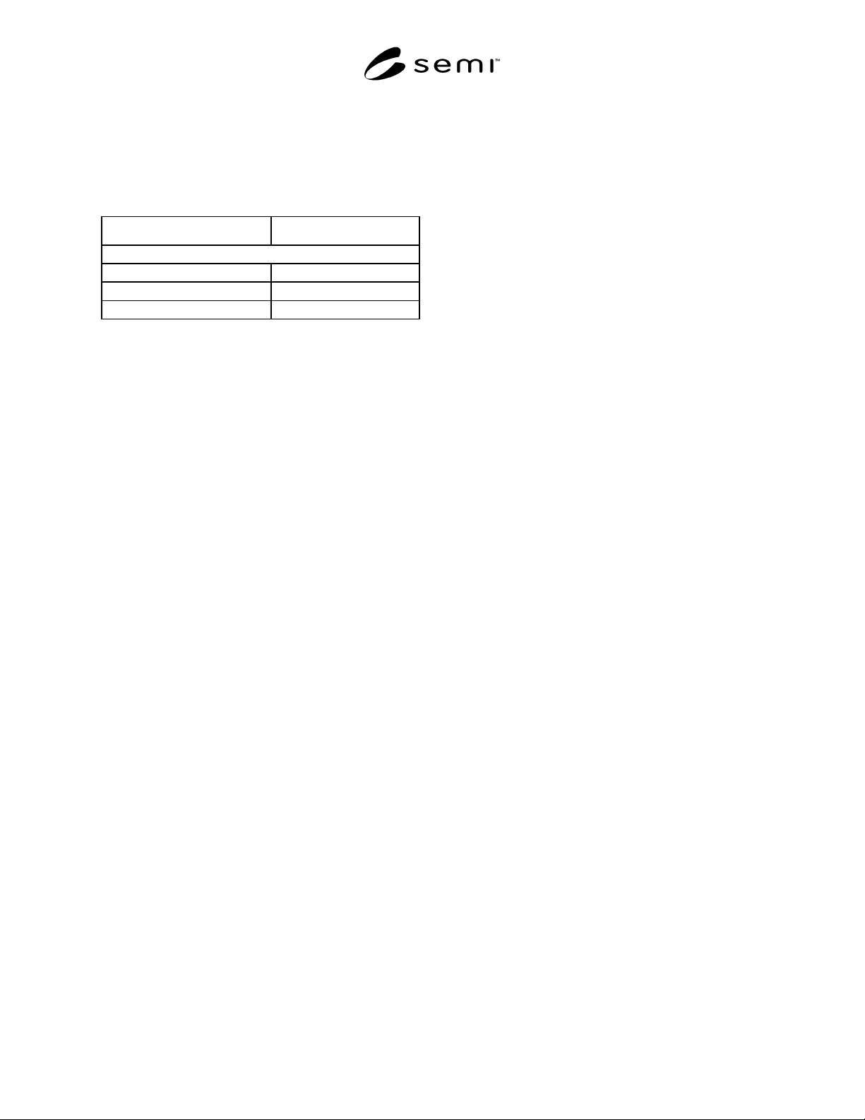
Table A1-1 Material Properties
Property
Ultra Low Thermal Expansion (ULTE)
Modulus of Elasticity 6.7–7.4 × 10
3
kg/mm
2
Poisson’s Ratio 0.16–0.19
Specific Gravity 2.18–2.20 g/cm
3
NOTICE: These standards do not purport to address
safety issues, if any, associated with their use. It is the
responsibility of the user of these standards to establish
appropriate safety and health practices and determine
the applicability of regulatory limitations prior to use.
SEMI makes no warranties or representations as to the
suitability of the standards set forth herein for any
particular application. The determination of the
suitability of the standard is solely the responsibility of
the user. Users are cautioned to refer to manufacturer’s
instructions, product labels, product data sheets, and
other relevant literature respecting any materials
mentioned herein. These standards are subject to
change without notice.
The user’s attention is called to the possibility that
compliance with this standard may require use of
copyrighted material or of an invention covered by
patent rights. By publication of this standard, SEMI
takes no position respecting the validity of any patent
rights or copyrights asserted in connection with any
item mentioned in this standard. Users of this standard
are expressly advised that determination of any such
patent rights or copyrights, and the risk of infringement
of such rights, are entirely their own responsibility.

SEMI P33-0998 © SEMI 1998 8
RELATED INFORMATION 1
TERMS AND DEFINITIONS
NOTE: This related information is not an official part of SEMI P33. The following terms and definitions are provided for
information only. The Microlithography-related definitions identified herein were compiled from the Terminology sections of the
Standards in the SEMI Microlithography Volume. The SEMI Microlithography Committee is currently updating all terminology
through the Microlithography Terms and Definitions Task Force, and will eventually include the updated terminology in the
SEMI Compilation of Terms.
SEMI makes no warranties or representations as to the
suitability of the terms and definitions set forth herein
for any particular application. The determination of the
suitability of the terms and definitions is solely the
responsibility of the user.
array rotation — the total array set rotated relative to
substrate edges.
cavity — in pellicle technology, an unfilled space
between the photomask and the optically transparent
film within the mounted pellicle frame area.
coherence, spatial — the correlation of the
electromagnetic fields at different points in space. Can
be achieved with a non-monochromatic source.
coherence, temporal — the correlation of
electromagnetic fields at different points in time but the
same point in space (related to the non-
monochromaticity of the source).
composite drawing — a large-scale drawing comprising
all geometric forms required for a single device,
arranged in proper relative positions. It is used as a
guide for manual cutting by Rubylith, or for a digitizing
guide for Computer Aided Design (see CAD). The set
of colored overlay films made as work progresses to the
reticle stage, can also be considered a composite,
suitable for checking design errors. (SYN: Master
Drawing, Engineering Drawing, Design Drawing.)
contact mask — in semiconductor fabrication, after the
major diffusions, gates, and other active areas have
been deposited, a glass insulating layer is placed over
the whole die. Small holes are etched through this glass
at points where the interconnecting metal conducts
must ‘contact’ the active areas. The mask that defines
these holes is characterized by many small squares
(~0.2–0.4 mil) scattered throughout the die area.
contact printing — a process of reproducing an original
by placing a photomask so that the coated side is in
contact with the photoresist (or emulsion) surface of the
area to be printed and then exposing the photoresist (or
emulsion).
cure, photoresist — the process of eliminating
undesirable properties of photoresists, such as
tackiness, softness, the tendency to flow, lack of
adhesion, etc.
dark area — an opaque area.
defect, gross photomask — a photomask defect that can
be easily seen with the naked eye or under
magnification no greater than 10×. Examples: large
scratches, cracks in the glass substrate, drying marks,
etc.
defect, photomask — any flaw or imperfection in the
opaque coating or functional pattern of a photomask
that will reproduce itself in a photoresist film to such a
degree that it is pernicious to the proper functioning of
the microelectronic device being fabricated.
degradation — reductions in image quality (measured
as resolution, edge acuity, dimensional shifts, defect
density, etc.) experienced in each generation of
reproduction, as compared to the original or preceding
generation. Generally, degradation increases with each
generation, in a predictable manner.
diffraction pattern, spatial — intensity variations of
light in the viewing plane caused by interference of
waves undergoing diffraction.
element — a member of the set that makes up the
photomask array; used either as a functional layer
member for the fabrication of a single, integrated circuit
or for test purposes. (Replaces chip, die, bar.)
emulsion — a suspension of a salt of silver in gelatin or
collodion that is coated onto a photoplate and is
exposed and developed to produce a photomask.
energy, minimum exposure — the energy corresponding
to the total integrated energy of actinic radiation
necessary to just completely render soluble a positive
photoresist for a given replacement film thickness or
just completely render insoluble a negative photoresist
for a given single resist film thickness.
energy, optimum exposure — the energy per square
centimeter corresponding to the total integrated energy
of actinic radiation necessary to accurately reproduce
photomask pattern dimensions in a photoresist of given
thickness after exposure and development.
etch resistance — the ability of a photomask coating or
protecting material, such as photoresist, in which the
pattern is imaged or photoprinted.