semi合集-English.pdf - 第5863页
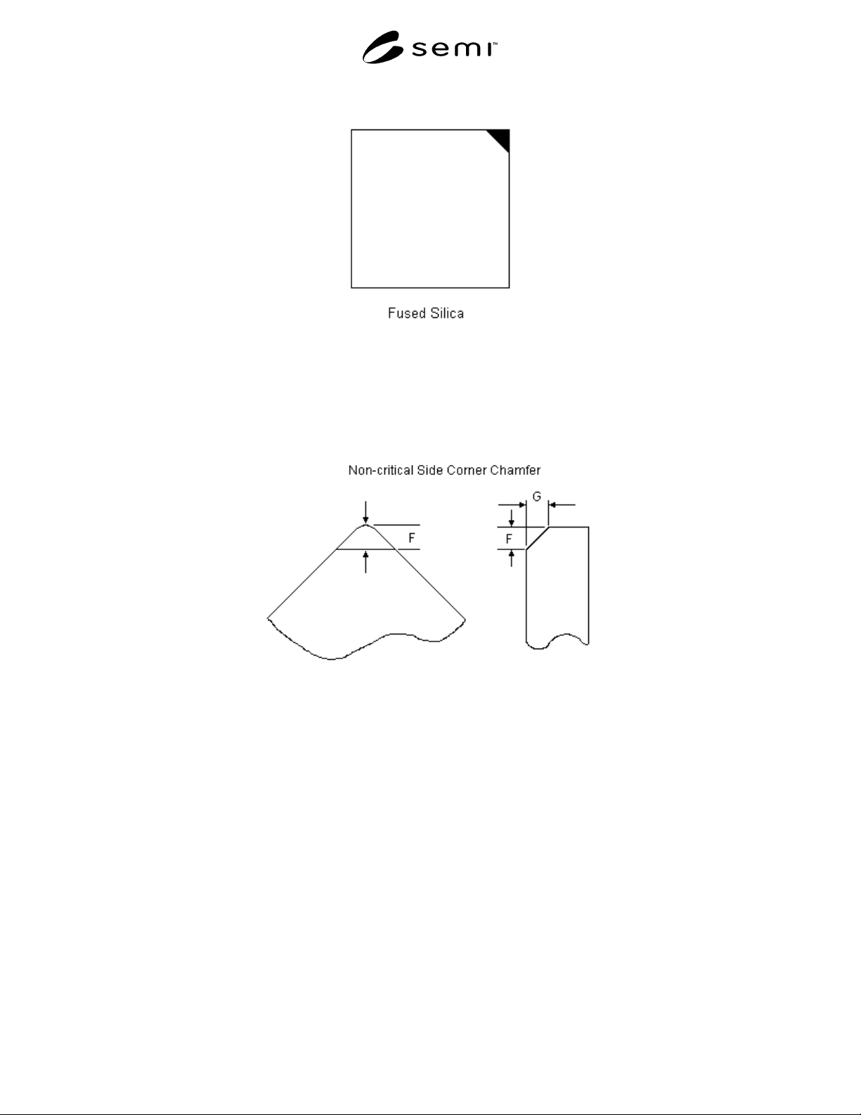
SEMI P34-0200 © SEMI 2000 6 Figure 5 Substrate Ide ntification by Co rner Chamfer (Non-critical Side) F = 1.5–2 .0 mm G = 0.6–1 .0 mm Figure 6 Dimension of Corner Cha mfer (Edge Chamfer Not Indicated)
SEMI P34-0200 © SEMI 20005
Table 4 Fused Silica Substrate Defect Limits
Bulk Defects Within the Visual Quality Area
Opaque Spots Bubble Total Defects (per cm
2
)Notes
> 1 µm> 1 µm
01, 2
≤ 1 µm ≤ 1 µm
0.0078
Surface Defects Within the Visual Quality Area
Residue Scratch Size Total Scratch
Defects
Sleek Size Total Sleek Defects
(per cm
2
)
Opaque Spot
Size
Total Opaque Spot
Defects (per cm
2
)
Critical side None
> 1.0 µm
0
> 1.0 µm
0
> 1.0 µm
0
≤ 1.0 µm
no limit
≤ 1.0 µm
0.0465
≤ 1.0 µm
0.0155
Non-critical side
> 1.0 µm
0
> 3.0 µm
0.0465
≤ 1.0 µm
no limit
≤ 3.0 µm
no limit
Defects Outside the Visual Quality Area
Defect Limit Total Number Notes
Edge Chips Radial Depth
≥ 0.76 mm
03
Peripheral Chord
≥ 0.76 mm
03
Other Shall be negotiated between user and
supplier.
Shall be negotiated between user and
supplier.
NOTES:
1. The size of internal defects is defined as 1/2 (long axis + short axis).
2. This table is based on the assumption that defects < 1 µm will fall outside the focal depth of the lens systems and should not print.
3. None of any size permitted that break the surface.
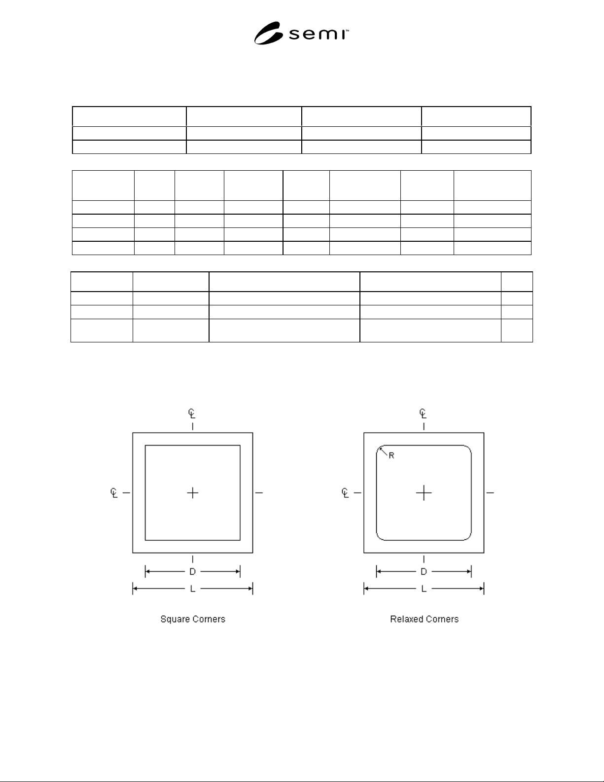
D ≥ 213 mm
R ≤ 6.5 mm (radius of curvature)
Figure 4a Figure 4b
Square Flatness Quality Area Relaxed Square Flatness Quality Area
SEMI P34-0200 © SEMI 2000 6
Figure 5
Substrate Identification by Corner Chamfer
(Non-critical Side)
F = 1.5–2.0 mm
G = 0.6–1.0 mm
Figure 6
Dimension of Corner Chamfer
(Edge Chamfer Not Indicated)
SEMI P34-0200 © SEMI 20007
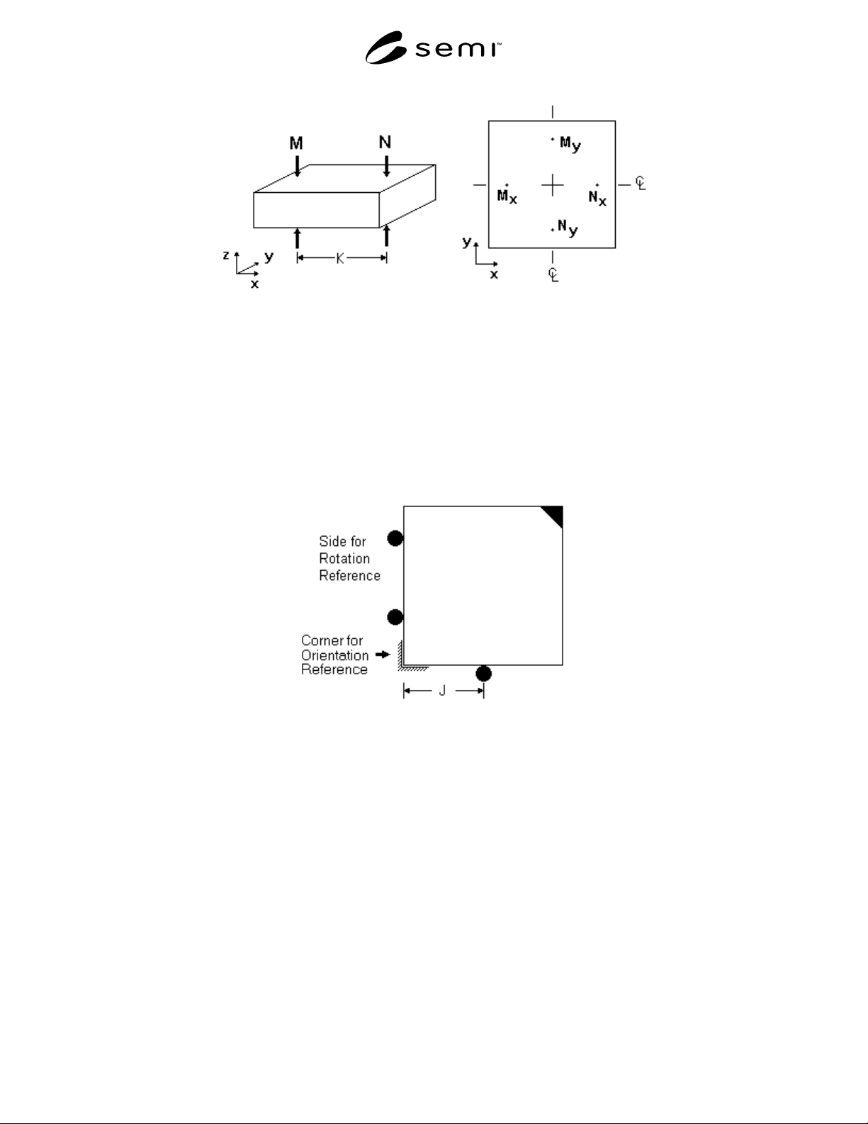
Parallelism = | N
i
– M
i
| for i = x, y
K = 0.7 × edge length N, M within flatness quality area
Figure 7
Measurements for Calculation of Parallelism
with Approximate Positions
J = 115 ± 15 mm
Figure 8
Corner Recommended for Orientation,
Diagonally Opposite of Chamfer (Non-critical Side Shown)