semi合集-English.pdf - 第5864页
SEMI P34-0200 © SEMI 2000 7 Paralle lism = | N i – M i | fo r i = x, y K = 0.7 × edge len gth N, M within f latness qu alit y area Figure 7 Measurements for Calculat ion of Parallelism with Approx i mate Pos itions J = 1…
SEMI P34-0200 © SEMI 2000 6
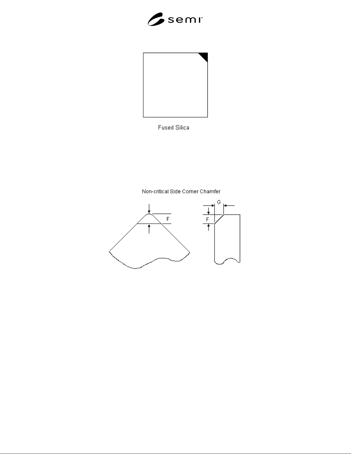
Figure 5
Substrate Identification by Corner Chamfer
(Non-critical Side)
F = 1.5–2.0 mm
G = 0.6–1.0 mm
Figure 6
Dimension of Corner Chamfer
(Edge Chamfer Not Indicated)
SEMI P34-0200 © SEMI 20007
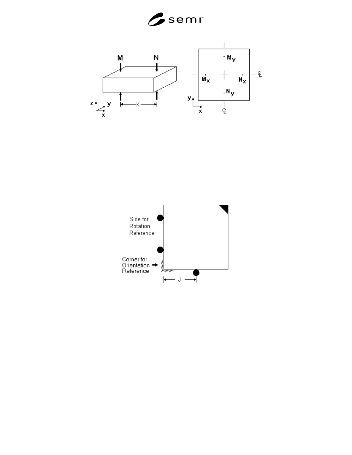
Parallelism = | N
i
– M
i
| for i = x, y
K = 0.7 × edge length N, M within flatness quality area
Figure 7
Measurements for Calculation of Parallelism
with Approximate Positions
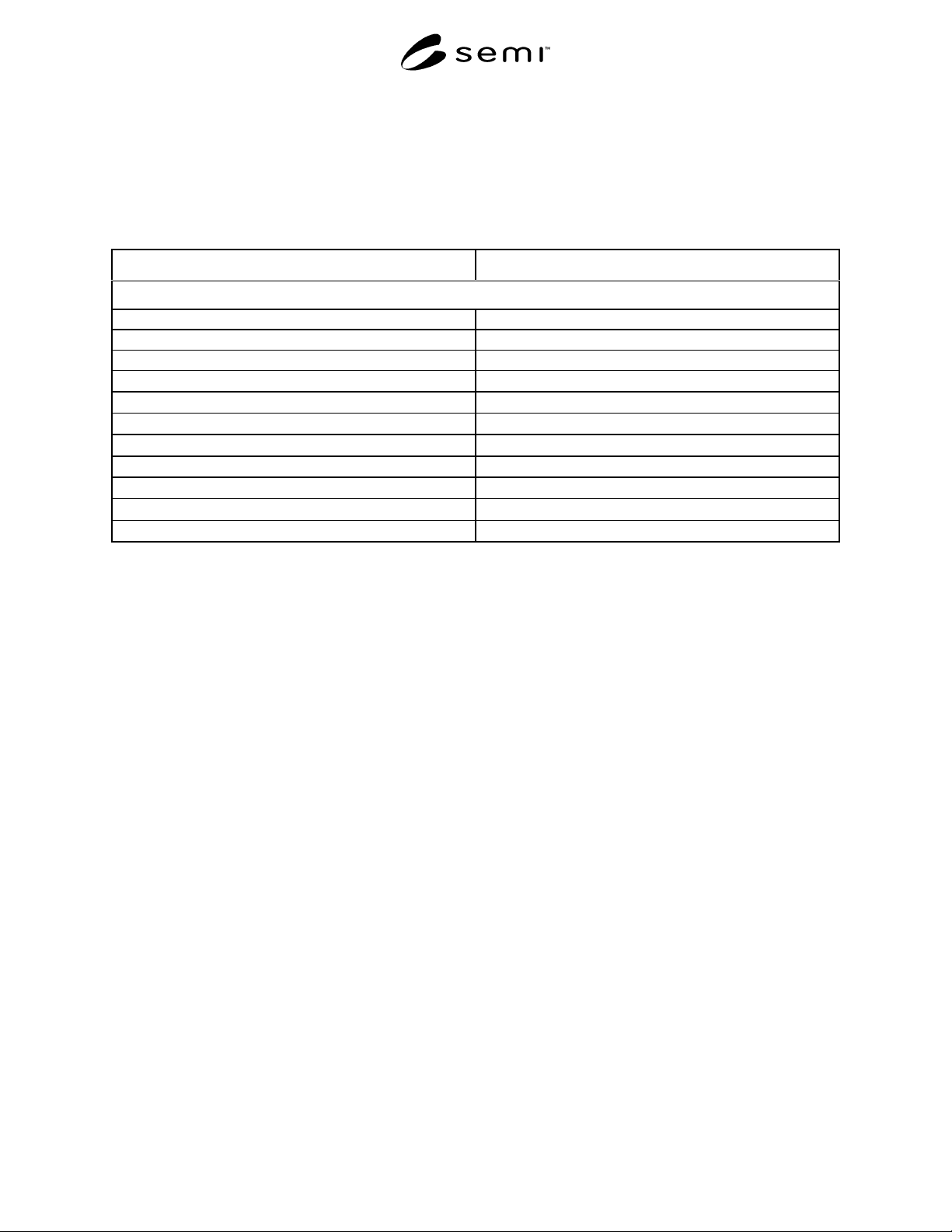
J = 115 ± 15 mm
Figure 8
Corner Recommended for Orientation,
Diagonally Opposite of Chamfer (Non-critical Side Shown)
SEMI P34-0200 © SEMI 2000 8
APPENDIX 1
PHOTOMASK FUSED SILICA PROPERTIES
NOTE: The material in this appendix is an official part of SEMI P34 and was approved by full letter ballot procedures on
September 3, 1999 by the North American Regional Standards Committee.
Table A1-1 Fused Silica Properties
Property
ULTRA LOW THERMAL EXPANSION (ULTE)
Modulus of Elasticity 65.7-72.6 GPa
Poisson's Ratio 0.16-0.19
Specific Gravity 2.18-2.20 g/cm
3
Index of Refraction @ λ = 436 nm
1.4667
Index of Refraction @ λ = 365 nm
1.4746
Index of Refraction @ λ = 248 nm
1.5086
Index of Refraction @ λ = 193 nm
1.5608
Thermal Optical Coefficient @ λ = 436 nm 10.6 ppm/°C @ 22°C
Thermal Optical Coefficient @ λ = 365 nm 11.2 ppm/°C @ 22°C
Thermal Optical Coefficient @ λ = 248 nm 14.2 ppm/°C @ 22°C
Thermal Optical Coefficient @ λ = 193 nm 20.6 ppm/°C @ 22°C
NOTE 1: Thermal Optical Coefficient is the same as Temperature Coefficient of Index of Refraction.
NOTICE: SEMI makes no warranties or representations as to the suitability of the standard set forth herein for any
particular application. The determination of the suitability of the standard is solely the responsibility of the user.
Users are cautioned to refer to manufacturer’s instructions, product labels, product data sheets, and other relevant
literature respecting any materials mentioned herein. These standards are subject to change without notice.
The user’s attention is called to the possibility that compliance with this standard may require use of copyrighted
material or of an invention covered by patent rights. By publication of this standard, SEMI takes no position
respecting the validity of any patent rights or copyrights asserted in connection with any item mentioned in this
standard. Users of this standard are expressly advised that determination of any such patent rights or copyrights, and
the risk of infringement of such rights, are entirely their own responsibility.
Copyright by SEMI® (Semiconductor Equipment and Materials
International), 3081 Zanker Road, San Jose, CA 95134. Reproduction o
f
the contents in whole or in part is forbidden without express written
consent of SEMI.