semi合集-English.pdf - 第5886页
SEMI P37-1102 © SEMI 2001, 2002 8 L D W Defect quality area L Figure 6 Definition of defect quality area on front side Table 5 Substrate Defect Limits p er Plate FRONTSIDE SURFACE DEFECTS IN THE DEFE CT QUALITY AREA Fron…
SEMI P37-1102 © SEMI 2001, 2002 7
P
1
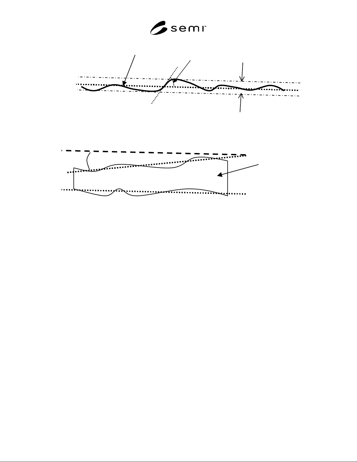
Mask substrate surface
Flatness error
Local slope
angle
Figure 4
Definition of Flatness Error and Local Slope Angle
P1 is the plane that minimizes maximum deviation of the surface.
α
Mask substrate
P
1
´
P
2
P
1
P
1
´ || P
1
Figure 5
Definition of Wedge Angle,
α
P
1
and P
2
are the planes that minimize the maximum deviation of the front and back surfaces, respectively.
SEMI P37-1102 © SEMI 2001, 2002 8
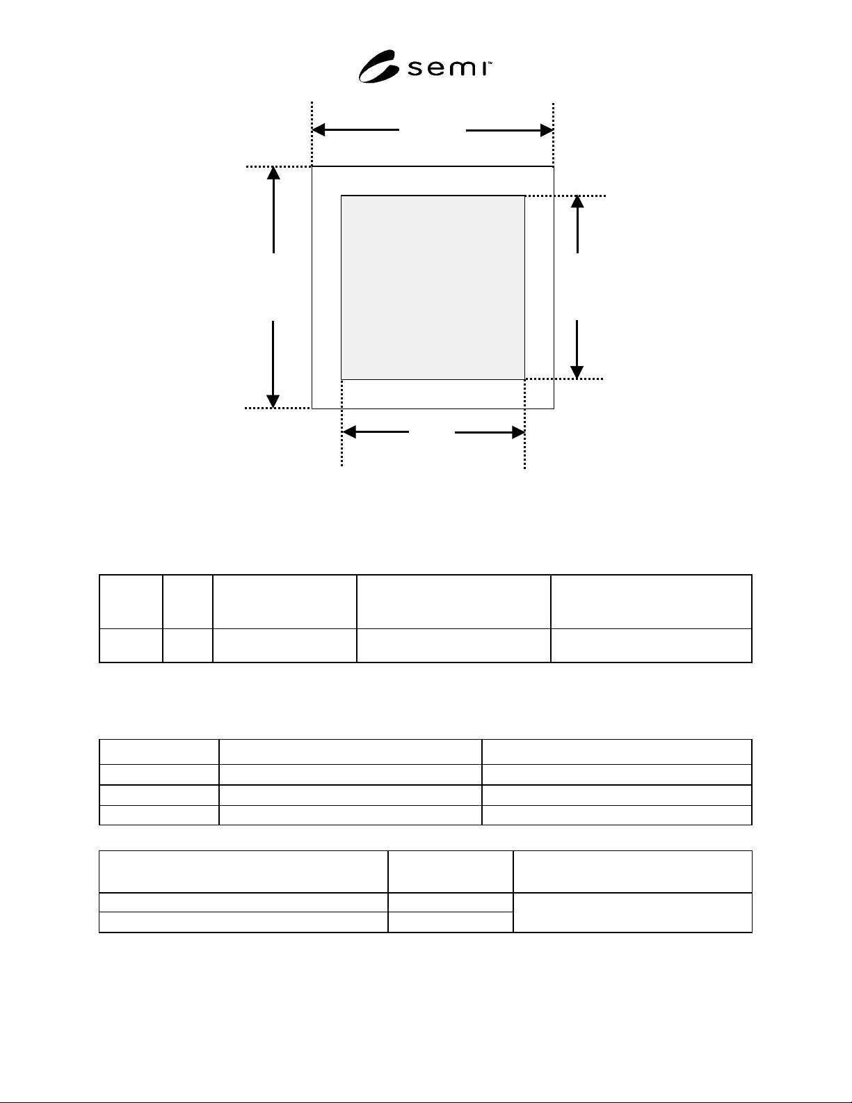
L
D
W
Defect
quality
area
L
Figure 6
Definition of defect quality area on front side
Table 5 Substrate Defect Limits per Plate
FRONTSIDE SURFACE DEFECTS IN THE DEFECT QUALITY AREA
Frontside
Residue
Total Scratch and Sleek
Defects > 1 nm in depth
(See Note 1.)
Total Localized Light Scatterers > 50
nm PSL equivalent size (per cm
2
)
(See Note 2.)
Total Localized Light Scatterers < 50
nm PSL equivalent size (per cm
2
)
(See Note 2.)
NZTE None 0 0 To be agreed upon between user and
supplier
NOTE 1: The maximum size for scratches and sleeks will be agreed upon between user and supplier.
NOTE 2: Localized light scatterers are any isolated features, such as particles or pits, on or in the substrate surface, resulting in increased light
scattering intensity relative to that of the surrounding substrate surface. PSL equivalent size means the detected defect appears to be the same
size as a polystyrene latex sphere examined under the same inspection conditions.
FRONTSIDE DEFECTS OUTSIDE THE DEFECT QUALITY AREA
Edge Chips Defect Limit Total Number
Radial Depth
≥ 0.76 mm
None
Peripheral Cord
≥ 0.76 mm
None
Other Shall be negotiated between vendor and supplier Shall be negotiated between vendor and supplier
BACKSIDE DEFECTS IN FLATNESS QUALITY AREA
Localized Light Scatterer Size (PSL equivalent)
(See Note 2.)
Total Total Number of Backside Scratches
(See Note 1.)
> 1.0 µm
0
≤ 1.0 µm
no limit
0
NOTE 1: The maximum size for scratches and sleeks will be agreed upon between user and supplier.
NOTE 2: Localized light scatterers are any isolated features, such as particles or pits, on or in the substrate surface, resulting in increased light
scattering intensity relative to that of the surrounding substrate surface. PSL equivalent size means the detected defect appears to be the same
size as a polystyrene latex sphere examined under the same inspection conditions.

SEMI P37-1102 © SEMI 2001, 2002 9
NOTICE: SEMI makes no warranties or representations as to the suitability of the standards set forth herein for any
particular application. The determination of the suitability of the standard is solely the responsibility of the user.
Users are cautioned to refer to manufacturer's instructions, product labels, product data sheets, and other relevant
literature, respecting any materials or equipment mentioned herein. These standards are subject to change without
notice.
By publication of this standard, Semiconductor Equipment and Materials International (SEMI) takes no position
respecting the validity of any patent rights or copyrights asserted in connection with any items mentioned in this
standard. Users of this standard are expressly advised that determination of any such patent rights or copyrights, and
the risk of infringement of such rights are entirely their own responsibility.