semi合集-English.pdf - 第5941页
SEMI P41-0304 E © SEMI 2004 1 SEMI P41-0304 E SPECIFICATION FOR MASK DEFECT DATA HANDLING WITH XML, BETWEEN DEFECT INSPECTION TOOLS, REPAIR TOOLS, AND REVIEW TOOLS This specification was technically approved by the Globa…
SEMI P40-1103 © SEMI 2003 6
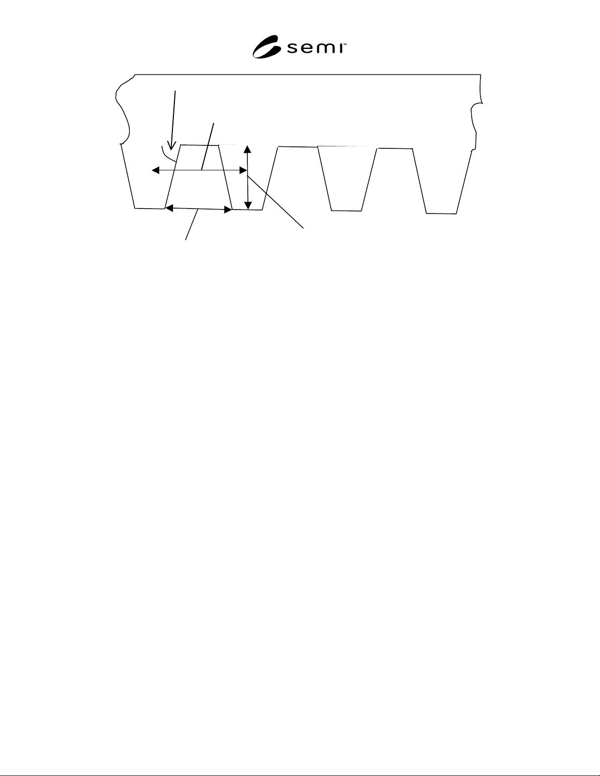
Pin sidewall angle
Chuck
Pin spacing, S
p
θ
Pin period, P
p
Pin height, H
p
Figure 5
Dimensions of Pins or Pedestals on the Chuck Surface
NOTICE: SEMI makes no warranties or representations as to the suitability of the standards set forth herein for any
particular application. The determination of the suitability of the standard is solely the responsibility of the user.
Users are cautioned to refer to manufacturer' s instructions, product labels, product data sheets, and other relevant
literature, respecting any materials or equipment mentioned herein. These standards are subject to change without
notice.
By publication of this standard, Semiconductor Equipment and Materials International (SEMI) takes no position
respecting the validity of any patent rights or copyrights asserted in connection with any items mentioned in this
standard. Users of this standard are expressly advised that determination of any such patent rights or copyrights, and
the risk of infringement of such rights are entirely their own responsibility.
Copyright by SEMI® (Semiconductor Equipment and Materials
International), 3081 Zanker Road, San Jose, CA 95134. Reproduction o
f
the contents in whole or in part is forbidden without express written
consent of SEMI.

SEMI P41-0304
E
© SEMI 2004 1
SEMI P41-0304
E
SPECIFICATION FOR MASK DEFECT DATA HANDLING WITH XML,
BETWEEN DEFECT INSPECTION TOOLS, REPAIR TOOLS, AND
REVIEW TOOLS
This specification was technically approved by the Global Micropatterning Committee and is the direct
responsibility of the Japanese Micropatterning Committee. Current edition approved by the Japanese
Regional Standards Committee on January 9, 2004. Initially available at www.semi.org February 2004; to be
published March 2004.
E
This standard was modified in September 2004 to correct editorial errors. Changes were made to Tables 2
and 3.
1 Purpose
1.1 This data structure specification uses the standard
XML format for defect information communication
between defect inspection tools, repair tools, and
review tools at the mask production floor.
1.1.1 Mutual use of the defect information between the
tools.
1.1.2 Optional usage by tools and systems other than
defect inspection, repair, and review tools.
1.2 The equipment suppliers who utilize this
standardized data structure can send and receive
required information, with no dependence on specific
software and specific hardware.
2 Scope
2.1 This standard can be applied to defect-related
information on photomasks for semiconductor
manufacturing.
2.2 This data structure defines the data hierarchy, the
tag name, and contents of an XML file, which are
transmitted. A particular database or a particular
programming language is not specified in this standard.
NOTICE: This standard does not purport to address
safety issues, if any, associated with its use. It is the
responsibility of the users of this standard to establish
appropriate safety and health practices and determine
the applicability of regulatory or other limitations prior
to use.
3 Limitations
3.1 This standard does not include the provision of
defect information for wafer fabs.
3.2 This standard does not specify particular schema.
3.3 This standard does not address the name space
issue.
4 Referenced Standards
4.1
World Wide Web Consortium Documents
1
Extensible Markup Language (XML) 1.0 (Second
Edition) — W3C,6 October 2000
(
http://www.w3.org/TR/2000/REC-xml-20001006)
4.2 JEITA Documents
2
Reticle Data Management Guideline Ver.1.0 (2001)
NOTICE: Unless otherwise indicated, all documents
cited shall be the latest published versions.
5 Terminology
5.1 Abbreviations and Acronyms
5.1.1 MDML — Mask Defect Markup Language
5.2 Definitions
5.2.1 defect inspection information — the information
gathered with mask defect inspection tools, such as
defect position and shape.
5.2.2 mask defect markup language — the name of the
XML file defined in this standard.
6 Requirements
6.1 This standard defines the layered structure of an
XML file, an element name, an attribute name and the
contents described in them. Users of this standard have
to define the style of the information described in an
element and an attribute, and it must be published.
6.2 The information on defect inspection information,
defect repair information, and defect review
information is treated as one file. The MDML data
item specifications defined in this standard are shown in
1 World Wide Web Consortium (W3C), ,Website:
http://www.w3c.org
2 Japanese Electronic and Information Technology Industries
Association, Tokyo Chamber of Commerce and Industry Bldg. 2-2,
Marunouchi 3-chome, Chiyoda-ku, Tokyo 100-0005, Japan. Website:
http://www.jeita.or.jp
SEMI P41-0304
E
© SEMI 2004 2
Tables 2–7. The columns in these tables are described
in the following sections. A layered structure is shown
in Figures 2–7. Figure 1 is explanation of Figures 2–7.
6.2.1 Item Name Column — The name with which the
data item is referenced.
6.2.2 Element or Attribute Column — Indicates
whether the item is an element or an attribute.
6.2.3 Mandatory or Optional Column — Indicates
whether the item is mandatory or optional.
6.2.4 Data Type Column — The type of data as defined
in Table 1.
Table 1 Data Types
Type Description
String A string of ASCII characters from 0 to 32767characters in length.
Integer A string of numeric characters (0 through 9) that represent an integer value.
Float A string representing a floating point value in exponent float.
6.2.5 Description Column – Description of what the data item is and what value restrictions it has
Table 2 Description of Basic Information Section
Item
Element or
attribute
Mandatory or
Optional
Data Type Description
MDML Element Mandatory - Route element.
data_no Attribute Optional Integer Management number in inspection tool.
date_stamp Attribute Optional String Generating time.
BasicInformation Element Mandatory - Top element of basic information.
MaskMaterialInformation Element Mandatory - Top element of material information.
MaskSize Element Mandatory - Mask size information.
unit Attribute Mandatory String Unit system.
shape Attribute Optional String Mask substrate shape.
MaskSize_X Element Mandatory Float Mask substrate size X.
MaskSize_Y Element Mandatory Float Mask substrate size Y.
MaskThickness Element Mandatory Float Mask substrate thickness.
MaskAbsorber Element Optional String Masking absorber.
DefectInspection Element Mandatory - Top element of basic information on defect
inspection.
preparation_date Attribute Optional String Generating time of basic information on defect
inspection.
InspectionTool Element Mandatory - Top element of defect inspection tool
information.
tool_name Attribute Optional String General name of tool.
tool_no Attribute Optional String Tool management number at mask fab.
ToolCoordinateInformation Element Mandatory - Top element of tool work stage coordinate
information. Subsequent structures are in Table
5. Refer to Figure 9.
InspectionMethod Element Mandatory String Defect inspection method.
PreparationOperator Element Optional String Operator name who created inspection basic
information.
ReferenceAreaDB Element Optional String When reusable basic information exists, the
reference address is to be described.
DirectionInformation Element Mandatory - Top element of direction for Mask and tool work
stage. Subsequent structures are in Table 6. Refer
to Figure 10.
AreaInformation Element Mandatory - Top element of inspection area information.
LensDistance Element Optional Float Lens separation at the die to die inspection.