semi合集-English.pdf - 第6034页
SEMI G3-90 © SEMI 1 980, 199 6 6 Layers sh all be designated by letter beginni ng with “A” as that layer nearest terminal in sertion plane. Layers, regardless of function, shall be designated b y succeeding letters , (B,…
SEMI G3-90 © SEMI 1980, 19965
3. Centrifuge — MIL-STD-883, Method 2001.2,
Condition E
4. Mechanical Shock — MIL-STD-883, Method
2002.2, Condition B
9.2.6 Sequence of Events and Incoming Testing —
During incoming inspection the sequence of testing
shall be:
1. Die Attach
2. Wire Bond
3. Pre-Seal Bond Pull
4. Seal
5. Environmental Test
6. Fine Leak
7. Gross Leak
8. Trim
9. Post-Seal Bond Pull
10.Radiography
11. Die Shear
12. Solderability
NOTE: An initial vendor qualification on the thermal and
electrical characteristics of the package may be performed.
The characteristics tested will be:
1. Insulation Resistance — MIL-STD-883, Method
1003, Test Condition D
2. Thermal Dissipation — MIL-STD-883, Method
1012
10 Packaging and Marking
10.1 Packaging — Containers selected shall be strong
enough and suitably designed to provide maximum
protection against crushing, spillage, and other forms of
damage to the container or its contents. Containers shall
afford protection of the contents to contamination from
exposure to excessive moisture or oxidation by gases.
Packaging materials shall be so selected to prevent any
contamination of the ceramic component parts with
paper fibers or organic particles.
10.2 Marking — The outer containers shall be clearly
marked to identify the user stock number, user purchase
order number, drawing number, quantity, and vendor
lot number.
11 Product Design
11.1 Leadframe Paddle Width and Standoff — (See
Figure 5.)
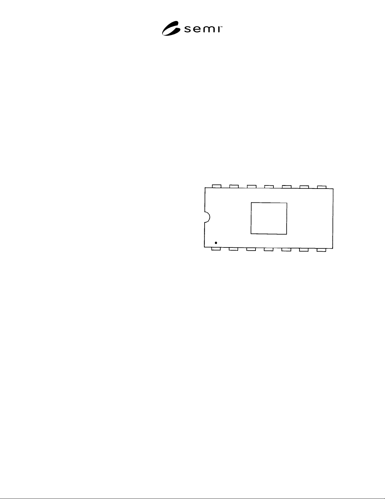
NOTE: A geometric symbol adjacent to an identifying lead
number 1 shall be considered appropriate for packages with
all leads isolated from the die attach.
NOTE: Lead number 14 is common to die attach surface and
is identified by placing this number where lead number 1 is
located.
11.1.1 Leadframe paddle width shall be 1.14 mm
(0.045") ± 0.178 mm (0.007").
11.1.2 Standoff shall be 1.02 mm ± 0.254 mm (0.040"
± 0.010").
11.1.3 Hole Diameter shall be 0.032" – 0.033" (0.813
mm – 0.838 mm).
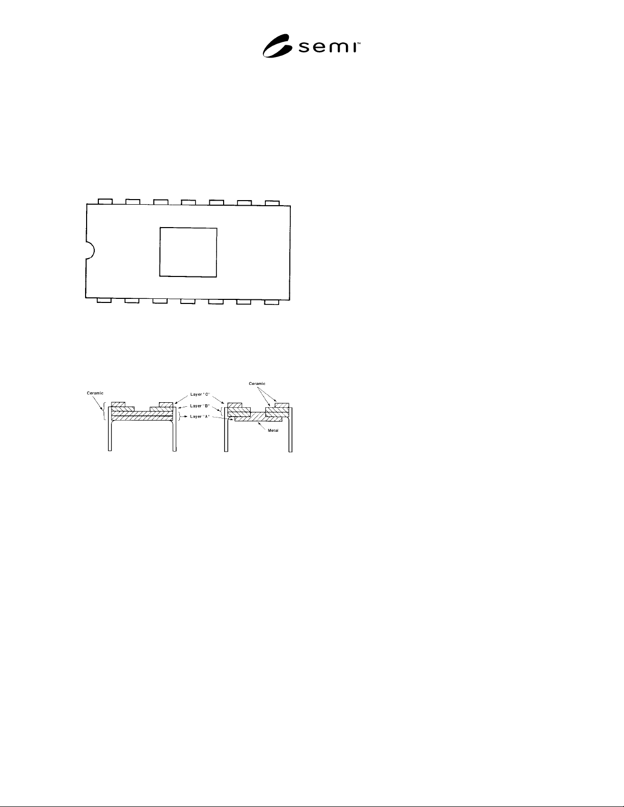
11.2 Substrate/Terminal Commonality on Sidebrazed
Laminate Packages — If no leads are common to the
die attach surface, the lead one identification shall be a
geometric symbol (Figure 6).
Figure 6
Lead Identification
SEMI G3-90 © SEMI 1980, 1996 6
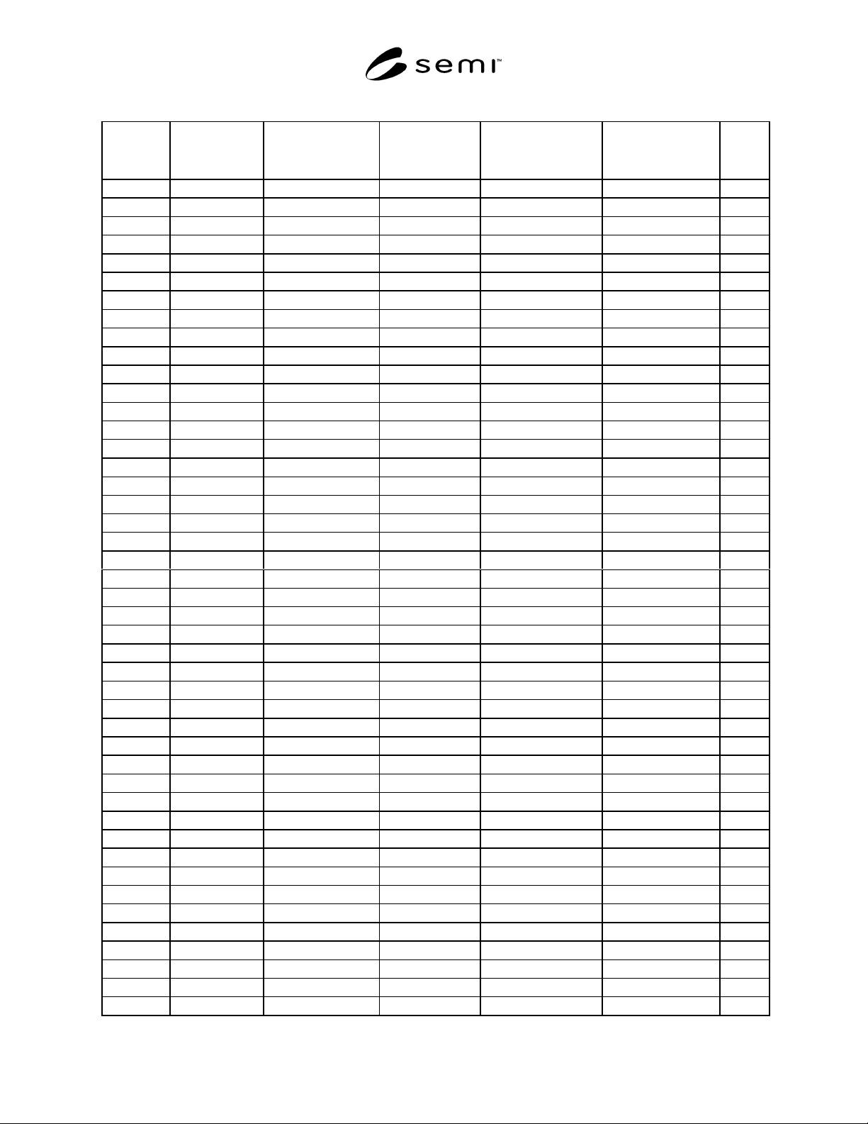
Layers shall be designated by letter beginning with “A”
as that layer nearest terminal insertion plane. Layers,
regardless of function, shall be designated by
succeeding letters, (B, C, D, etc.) as being progressively
remote from the terminal insertion plane.
Should any lead be common to the die attach surface,
that lead number will serve both as lead one
identificationand as an indicator as to the lead that is
common to the die attach surface (Figure 7).
14
Figure 7
Lead Identification
11.3 Sidebraze Ceramic Package Layer Design —
(See Figure 8).
Figure 8
Layer Designation
SEMI G3-90 © SEMI 1980, 19967
Table 1 Sidebrazed Laminate Packages Dimensions and Tolerance Requirements
Desription Package Length
Package Width
(Inc. Leadframe)
Package Thickness
Min. Max.
Cavity Length
(Measured at Cavity
Bottom)
Cavity Width
(Measured at Cavity
Bottom) Units
8MSI 0.520 ± 0.008 0.310 + 0.010 - 0.015 0.076 – 0.094 0.180 ± 0.005 0.150 ± 0.005 in
13.21 ± 0.203 7.87 + 0.254 - 0.381 1.93 – 2.39 4.57 ± 0.127 3.81 ± 0.127 mm
8LSI 0.520 ± 0.008 0.310 + 0.010 – 0.015 0.076 - 0.094 0.220 ± 0.005 0.175 ± 0.005 in
13.21 ± 0.203 7.87 + 0.254 - 0.381 1.93 - 2.39 5.59 ± 0.127 4.45 ± 0.127 mm
8VLSI 0.520 ± 0.008 0.310 + 0.010 – 0.015 0.076 - 0.094 0.260 ± 0.005 0.175 ± 0.005 in
13.21 ± 0.203 7.87 + 0.254 - 0.381 1.93 - 2.39 6.60 ± 0.127 4.45 ± 0.127 mm
14MSI 0.750 ± 0.010 0.310 + 0.010 – 0.015 0.076 – 0.094 0.180 ± 0.005 0.150 ± 0.005 in
19.05 ± 0.254 7.87 + 0.254 - 0.381 1.93 – 2.39 4.57 ± 0.127 3.81 ± 0.127 mm
14LSI 0.750 ± 0.010 0.310 + 0.010 – 0.015 0.076 - 0.094 0.220 ± 0.006 0.175 ± 0.005 in
19.05 ± 0.254 7.87 + 0.254 - 0.381 1.93 - 2.39 5.59 ± 0.152 4.45 ± 0.127 mm
14VLSI 0.750 ± .010 0.310 + 0.010 – 0.015 0.076 – 0.094 0.260 ± 0.006 0.175 ± 0.005 in
19.05 ± 0.254 7.87 + 0.254 - 0.381 1.93 – 2.39 6.60 ± 0.152 4.45 ± 0.127 mm
16MSI 0.800 ± 0.010 0.310 + 0.010 – 0.015 0.076 - 0.094 0.220 ± 0.006 0.175 ± 0.005 in
20.32 ± 0.254 7.87 + 0.254 - 0.381 1.93 - 2.39 5.59 ± 0.152 4.45 ± 0.127 mm
16LSI 0.800 ± 0.010 0.310 + 0.010 – 0.015 0.076 – 0.094 0.240 ± 0.006 0.175 ± 0.005 in
20.32 ± 0.254 7.87 + 0.254 - 0.381 1.93 – 2.39 6.10 ± 0.152 4.45 ± 0.127 mm
16VLSI 0.800 ± 0.010 0.310 + 0.010 – 0.015 0.076 - 0.094 0.320 ± 0.007 0.175 ± 0.005 in
20.32 ± 0.254 7.87 + 0.254 - 0.381 1.93 - 2.39 8.13 ± 0.178 4.45 ± 0.127 mm
18MSI 0.900 ± 0.010 0.310 + 0.010 – 0.015 0.076 – 0.094 0.220 ± 0.006 0.175 ± 0.005 in
22.86 ± 0.254 7.87 + 0.254 - 0.381 1.93 – 2.39 5.59 ± 0.152 4.45 ± 0.127 mm
18LSI 0.900 ± 0.010 0.310 + 0.010 – 0.015 0.076 - 0.094 0.265 ± 0.006 0.175 ± 0.005 in
22.86 ± 0.254 7.87 + 0.254 - 0.381 1.93 - 2.39 6.73 ± 0.152 4.45 ± 0.127 mm
18VLSI 0.900 ± 0.010 0.310 + 0.010 – 0.015 0.076 – 0.094 0.320 ± 0.007 0.175 ± 0.005 in
22.86 ± 0.254 7.87 + 0.254 - 0.381 1.93 – 2.39 8.13 ± 0.178 4.45 ± 0.127 mm
20MSI 1.000 ± 0.010 0.310 + 0.010 – 0.015 0.076 - 0.094 0.215 ± 0.005 0.175 ± 0.005 in
24.89 ± 0.254 7.87 + 0.254 - 0.381 1.93 - 2.39 5.46 ± 0.127 4.45 ± 0.127 mm
20LSI 1.000 ± 0.010 0.310 + 0.010 – 0.015 0.076 – 0.094 0.265 ± 0.006 0.175 ± 0.005 in
24.89 ± 0.254 7.87 + 0.254 - 0.381 1.93 – 2.39 6.73 ± 0.152 4.45 ± 0.127 mm
20VLSI 1.000 ± 0.010 0.310 + 0.010 – 0.015 0.076 - 0.094 0.320 ± 0.007 0.175 ± 0.005 in
24.89 ± 0.254 7.87 + 0.254 - 0.381 1.93 - 2.39 8.13 ± 0.178 4.45 ± 0.127 mm
22MSI 1.08 ± 0.011 0.410 + 0.010 – 0.015 0.076 – 0.094 0.250 ± 0.006 0.220 ± 0.006 in
27.34 ± 0.279 10.41 + 0.254 - 0.381 1.93 – 2.39 6.35 ± 0.152 5.59 ± 0.152 mm
22LSI 1.08 ± 0.011 0.410 + 0.010 – 0.015 0.076 - 0.094 0.285 ± 0.006 2.20 ± 0.006 in
27.34 ± 0.279 10.41 + 0.254 - 0.381 1.93 - 2.39 7.24 ± 0.152 5.59 ± 0.152 mm
22VLSI 1.08 ± 0.011 0.410 + 0.010 – 0.015 0.076 – 0.094 0.280 ± 0.006 0.260 ± 0.006 in
27.34 ± 0.279 10.41 + 0.254 - 0.381 1.93 - 2.39 7.11 ± 0.152 6.60 ± 0.152 mm
24MSI 1.20 ± 0.012 0.610 + 0.010 – 0.015 0.076 - 0.094 0.250 ± 0.006 0.250 ± 0.006 in
30.48 ± 0.305 15.49 + 0.254 - 0.381 1.93 - 2.39 6.35 ± 0.152 6.35 ± 0.152 mm
24LSI 1.20 ± 0.012 0.610 + 0.010 – 0.015 0.076 – 0.094 0.305 ± 0.010 0.305 ± 0.010 in
30.48 ± 0.305 15.49 + 0.254 - 0.381 1.93 – 2.39 7.75 ± 0.254 7.75 ± 0.254 mm
24VLSI 1.20 ± 0.012 0.610 + 0.010 – 0.015 0.076 - 0.094 0.340 ± 0.008 0.340 ± 0.008 in
30.48 ± 0.305 15.49 + 0.254 - 0.381 1.93 - 2.39 8.64 ± 0.203 8.64 ± 0.203 mm
28MSI 1.40 ± 0.014 0.610 + 0.010 – 0.015 0.076 – 0.094 0.250 ± 0.006 0.250 ± 0.006 in
35.56 ± 0.356 15.49 + 0.254 - 0.381 1.93 – 2.39 6.35 ± 0.152 6.35 ± 0.152 mm
28LSI 1.40 ± 0.014 0.610 + 0.010 – 0.015 0.076 - 0.094 0.305 ± 0.010 0.305 ± 0.010 in