semi合集-English.pdf - 第6048页
SEMIG4-0302 © SEMI 1982, 2002 12 NOTICE: T hese stan dards do not purport to addres s safety issues, if an y, associated w ith their use. It is the responsibility of the user of th ese standard s to establish appr opriat…
SEMI G4-0302 © SEMI 1982, 2002 11
APPENDIX 3
TEST METHOD FOR SLIT STRAIN OF LEADFRAME STRIPS USED
FOR STAMPING
NOTE: The material in this appendix is an official part of SEMI G4.
A3-1 Preface
A3-1.1 The method is used to evaluate the edge stress caused by slitting.
A3-1.2 This method is applied to thickness between 0.1 mm and 0.3 mm.
A3-2 Evaluation Method
A3-2.1 Equipment — Tool microscope (×100).
A3-2.2 Procedure
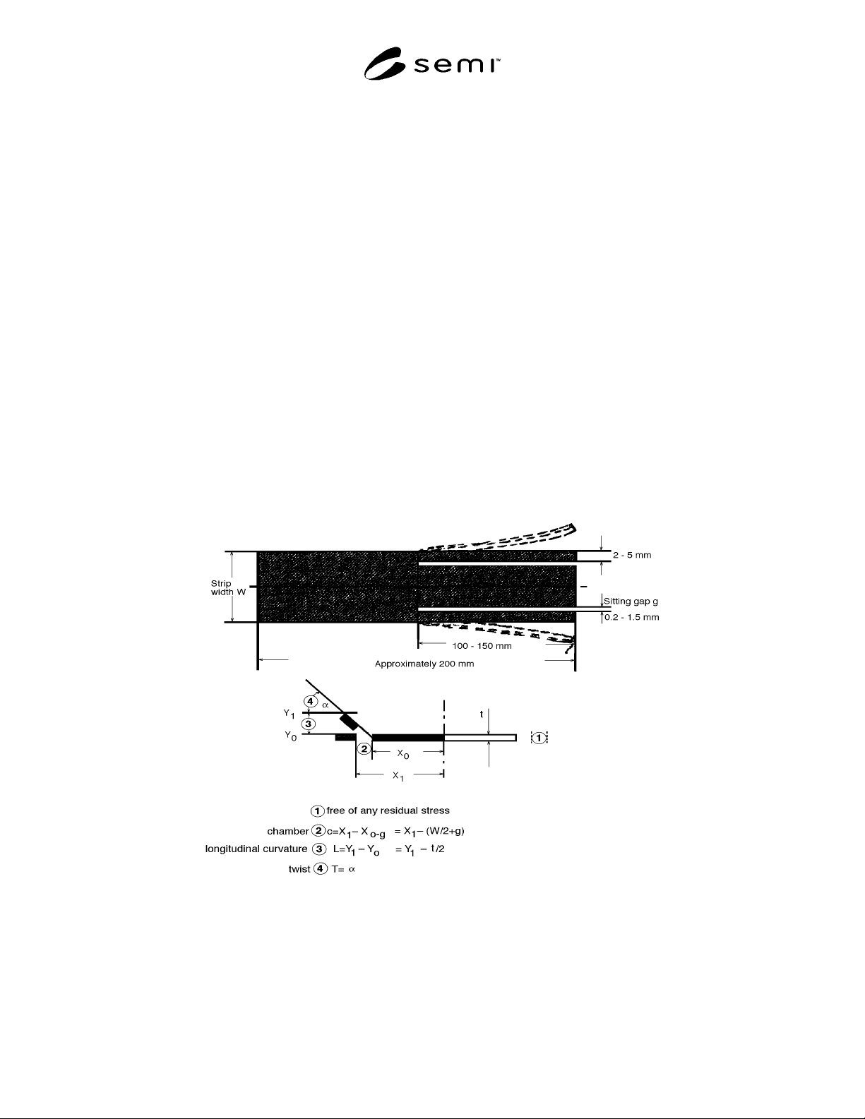
A3-2.2.1 A test piece of approximately 200 mm length is sawn, stamped, etched, wire cut, refined cut, etc., over a
length of 100–150 mm parallel to the rolling direction of a distance of 2–5 mm from the edge of the strip. (See
Figure A1-7.)
A3-2.2.2 The dislocation of the outer strips relative to the plane of the test piece measured as camber c, longitudinal
curvature L, and twist T characterize the internal edge stress. (Note 1)
Note 1: The details of the test method and the maximum admissible values of c, L, and T shall be agreed between purchaser and
supplier.
Figure A1-7
Test Method of Slit Stress

SEMIG4-0302 © SEMI 1982, 2002 12
NOTICE: These standards do not purport to address safety issues, if any, associated with their use. It is the
responsibility of the user of these standards to establish appropriate safety and health practices and determine the
applicability of regulatory limitations prior to use. SEMI makes no warranties or representations as to the suitability
of the standards set forth herein for any particular application. The determination of the suitability of the standard is
solely the responsibility of the user. Users are cautioned to refer to manufacturer’s instructions, product labels,
product data sheets, and other relevant literature respecting any materials mentioned herein. These standards are
subject to change without notice.
The user’s attention is called to the possibility that compliance with this standard may require use of copyrighted
material or of an invention covered by patent rights. By publication of this standard, SEMI takes no position
respecting the validity of any patent rights or copyrights asserted in connection with any item mentioned in this
standard. Users of this standard are expressly advised that determination of any such patent rights or copyrights, and
the risk of infringement of such rights, are entirely their own responsibility.
Copyright by SEMI® (Semiconductor Equipment and Materials
International), 3081 Zanker Road, San Jose, CA 95134. Reproduction o
f
the contents in whole or in part is forbidden without express writte
n
consent of SEMI.

SEMI G5-87 © SEMI 1980, 19961
SEMI G5-87
STANDARD FOR CERAMIC CHIP CARRIERS
1 Scope
This specification defines the acceptance criteria for co-
fired, ceramic chip carriers both leaded and lead-less.
2 Applicable Documents
2.1 ANSI Specification
1
S Y 14.5 — Dimensioning and Tolerancing
2.2 Federal Specification
2
QQ-N-290 — Nickel Plating
2.3 JEDEC Specification
3
Pub. No. 95 — Registered and Standard Outline for
Solid State Products
2.4 Military Specifications
4
MIL-STD-105 — Sampling Procedures and Tables for
Inspection by Attributes
MIL-STD-883 — Test Methods and Procedures for
Microelectronics
MIL-STD-7883 — Brazing
MIL-M-38510 — General Specification for
Microcircuits
MIL-STD-45204 — Gold Plating, Electrodeposited
2.5 SEMI Specifications
SEMI G8 — Test Method for Gold Plating Quality
SEMI G25 — Test Method for Measuring the
Resistance of Package Leads
SEMI G6 — Test Method for Seal Ring Flatness
3 Selected Definitions
braze — An alloy with a melting point equal to or
greater than 600°C.
castellation — That series of ribs and metallized
indentations that define edge contact regions (see
Figure 1).
1 ANSI, 1430 Broadway, New York, NY 10018
2 Military Standards, Naval Publications and Form Center, 5801
Tabor Ave., Philadelphia, PA 19120
3 JEDEC, 2001 Eye Street, N.W., Washington, D.C. 20006
4 General Services Administrator, 4th and D Streets, SW, Room
6039, Washington, D.C. 20407
fired — A process or technology to manufacture
products in which the ceramic and refractory
metallization are fired simultaneously.
contact pad — That metallized pattern that provides
mechanical or electrical connection to the external
circuitry.
die attach surface — See Figure 3.
footprint — Contact pad pattern.
layer — A dielectric sheet with or without metallization
that performs a discrete function as a part of the
package.
lead offset — Alignment of leads across the package.
pullback — The linear distance between the edge of the
ceramic and the first measurable metallization and/or
glass interface (see Figures 4 and 5).
rundown — See Figures 4 and 5.
seal-area — A dimensional outline area designated for
either metallization or bare ceramic to provide a surface
area for sealing (see Figure 3).
terminal — Case outline at point of entry or exit of an
electrical contact.
TIR — Total Indicator Reading.
4 Ordering Information
Purchase order for ceramic chip carriers furnished to
this specification shall include the following items:
1. Quantity
2. Drawing — The drawing(s) for ceramic chip
carriers shall specify the following information:
a. Drawing number and revision level.
b. Number of terminals and terminal center line
spacing.
c. Lead material and dimensions.
d. Critical material properties.
e. Type and thickness of plating.
f. Package dimensions per ANSI Y14.5.
g. Internal bonding patterns.
h. Minimum exposed metallized bond finger length
and width.