semi合集-English.pdf - 第6053页
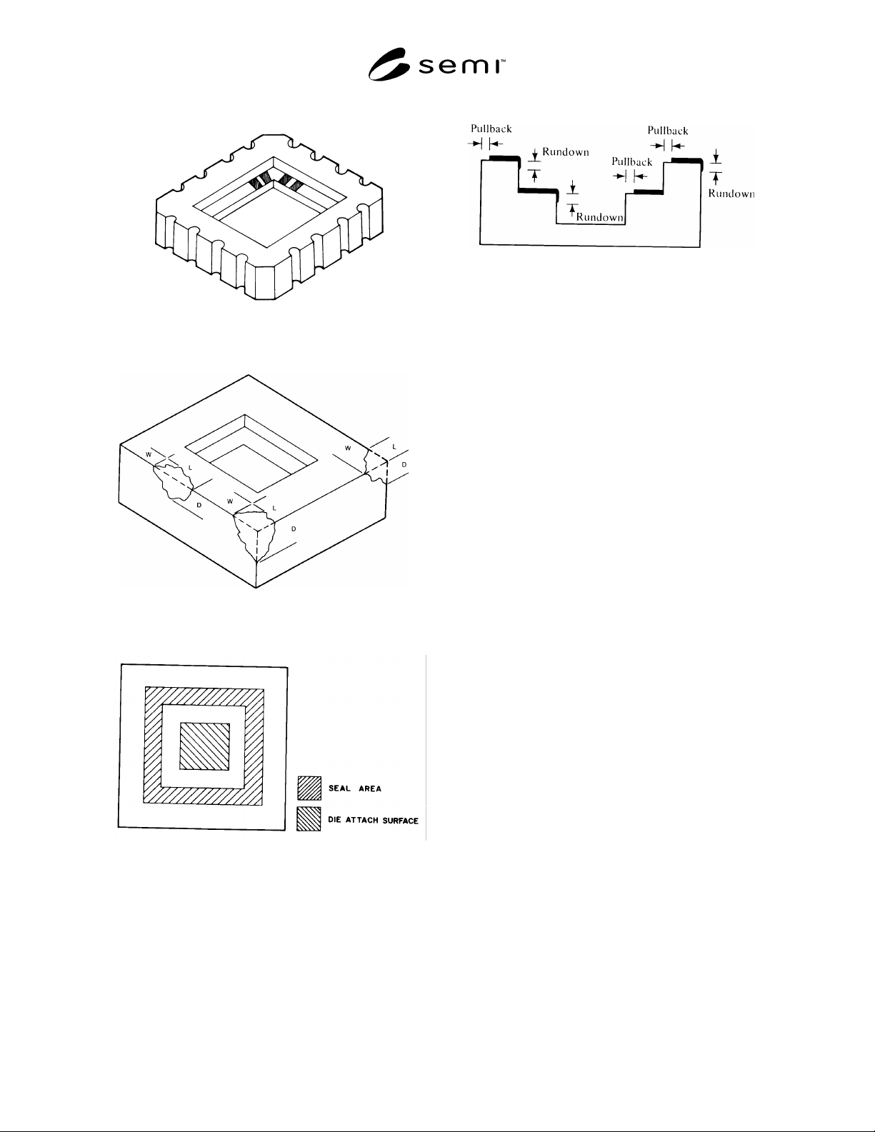
SEMI G5-87 © SEMI 1 980, 199 6 5 Figure 1 Castellations Figure 2 Chip Illustration Figure 3 Die Attach Surface and Seal Area Figure 4 Metallizat ion Misa lignment

SEMI G5-87 © SEMI 1980, 1996 4
8.3.3 Pattern Definitions (Cavity Packages) — (See
Figure 4.)
8.3.3.1 Seal Plane Rundown — internal cavity — Not
to exceed 25% of the cavity layer thickness.
8.3.3.2 External to the Cavity — Separation shall not
be less than 0.254 mm (0.010") or 50% of the design
width, whichever is less.
8.3.3.3 Wire Bond Finger Pullback — Not to exceed
maximum from the cavity edge. The minimum exposed
lead length must meet the dimension per applicable
drawing.
8.3.3.4 Wire Bond Finger Rundown — Not to exceed
25% of the ceramic layer thickness or 0.127 mm
(0.005"), whichever is smaller.
8.3.4 Pattern Separation — Minimum shall not be
reduced by more than 50% of the design.
8.4 Lead Attachment
8.4.1 Voids in Braze — 66% of the braze fillet must be
void-free.
8.4.2 Lead Alignment — Misalignment leads to braze
pads — The leads shall not overhang braze pads.
8.4.2.1 Lead Offset — To be specified on user
drawing. Lead center lines must be aligned to within
.178 mm (.007").
8.4.2.2 Lead-to-Lead Misalignment — To exceed ±
10% of nominal lead spacing.
8.4.2.3 Dimensional Criteria — To be specified on
user drawing.
9 Sampling
Sample sizes must meet requirements of MIL-STD-105
or MIL-M-38510 as agreed to between vendor and
customer. Single, double, or multiple samples may be
used.
10 Test Methods
10.1 Mechanical, Electrical, and Thermal Test
Methods — Per MIL-STD-883, unless otherwise noted.
10.1.1 Gold plating thickness shall conform to MIL-
STD-45204. Gold thickness may be determined using
the Beta Backscatter Radiation Method or X-Ray
Fluorescence.
10.1.2 Nickel plating shall conform to MIL-STD-
45204. Nickel thickness may be determined using the
Beta Backscatter Radiation Method.
10.1.3 Seal Ring Flatness — See SEMI G6.
10.1.4 Electrical Trace Resistance — See SEMI G25.
10.1.5 Gold Plating Quality — See SEMI G8.
10.1.6 Die Shear — Destructive — Method 2019.
10.1.7 Wire Bond — Method 2011, Condition D.
Reject for bonds which cause plating to lift from the
base metal of the die attach surface or bonding fingers.
10.1.8 Temperature Cycle — Method 1010, Condition
C.
10.1.9 Thermal Shock — Method 1011, Condition C.
10.1.10 Constant Acceleration — Method 2001,
Condition E.
10.1.11 Mechanical Shock — Method 2002, Condition
B.
10.1.12 Insulation Resistance — Method 1003.
10.1.13 Internal Water Vapor Content — Method
1018.
10.1.14 Hermeticity — Method 1014, Conditions A,
B, and C. The hermetic integrity of the package must be
maintained after all environmental testing.
10.1.15 Lead Integrity — Method 2004, Condition B.
10.1.16 Solderability — 2003.
10.1.17 Moisture Resistance Testing — Method 1004.
11 Packaging and Marking
11.1 Packaging — Containers selected shall be strong
enough, and suitably designed, to provide maximum
protection against crushing, spillage, and other forms of
damage to the container or its contents. Containers shall
afford protection of the contents to contamination from
exposure to excessive moisture or oxidation by gases.
Packaging materials shall be so selected to prevent any
contamination of the ceramic component parts with
paper fibers or organic particles. Regardless of
packaging, all parts should be cleaned before testing or
use.
11.2 Marking — The outer containers shall be clearly
marked identifying:
1. Vendor Part #
2. Customer Part #
3. Quantity
4. Date
5. Vendor Lot #
6. User P.O. number (optional)
7. Drawing number (optional)
SEMI G5-87 © SEMI 1980, 19965
Figure 1
Castellations
Figure 2
Chip Illustration
Figure 3
Die Attach Surface and Seal Area
Figure 4
Metallization Misalignment
SEMI G5-87 © SEMI 1980, 1996 6
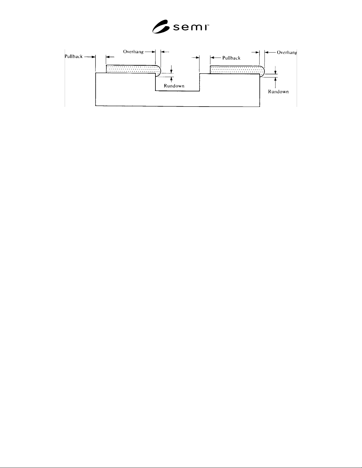
Figure 5
Glass Misalignment
NOTICE: These standards do not purport to address safety issues, if any, associated with their use. It is the
responsibility of the user of these standards to establish appropriate safety and health practices and determine the
applicability of regulatory limitations prior to use. SEMI makes no warranties or representations as to the suitability
of the standards set forth herein for any particular application. The determination of the suitability of the standard is
solely the responsibility of the user. Users are cautioned to refer to manufacturer’s instructions, product labels,
product data sheets, and other relevant literature respecting any materials mentioned herein. These standards are
subject to change without notice.
The user’s attention is called to the possibility that compliance with this standard may require use of copyrighted
material or of an invention covered by patent rights. By publication of this standard, SEMI takes no position
respecting the validity of any patent rights or copyrights asserted in connection with any item mentioned in this
standard. Users of this standard are expressly advised that determination of any such patent rights or copyrights, and
the risk of infringement of such rights, are entirely their own responsibility.
Copyright by SEMI® (Semiconductor Equipment and Materials
International), 3081 Zanker Road, San Jose, CA 95134. Reproduction o
f
the contents in whole or in part is forbidden without express written
consent of SEMI.