semi合集-English.pdf - 第6104页
SEMI G21-94 © SEMI 198 0, 1996 1 SEMI G21-94 SPECIFIC A TI ON FOR PLATING INTEGRATED CIRCUIT LEADFRAMES 1 Preface 1.1 Pur pose — This specification d e ta ils the requirements for plating la yers on leadframes intended f…

SEMI G20-96 © SEMI 1980, 19963
5.4.3 Appearance — Smooth and continuous and
semi-bright with minimum discoloration as measured,
in accordance with SEMI G55.
5.4.4 Hardness — Hardness shall be between 90 and
135 on the Brinell Hardness Scale, in accordance with
ASTM E 10.
5.4.5 Additional Processing
5.4.5.1 Due to chemical reactions, silver electroplated
surfaces should be protected from sulfur and sulfur
bearing materials such as note paper, cardboard, and
other like materials. Sulfur-free papers shall be used for
packing.
5.4.5.2 Prior to shipment to a user, devices with silver
electroplated leads shall have the silver removed and
replaced with tin lead coated leads, unless accepted by
contract.
5.5 Gold Electroplate
5.5.1 Composition — Gold plating shall be applied in
accordance with MIL-G-45204 in any and all of the
following grades depending on application.
Type I - 99.7 Percent minimum
Type II - 99.0 Percent minimum
Type III - 99.9 Percent minimum
NOTE 1: Type II is suitable for socketing application only.
5.5.2 Thickness — Shall be a minimum of 1.25
micrometers (50 microinches) as measured on the
major flat of the leads.
5.5.3 Appearance — Appearance of surface shall be
smooth and continuous. Attributes and defects are
specified in MIL-G-45204 (workmanship paragraph).
5.5.4 Purity — Composition limits are as specified in
Section 5.5.1 above. Individual metallics in the deposit
shall not exceed 0.1%. Metallic hardening agents,
purposely added to adjust a plating bath to specified
hardness, are not considered as impurities.
5.5.5 Hardness — Depending on Type and
Application, hardness is specified, using Knoop
indenter in the following categories (testing shall be in
accordance with ASTM E 384):
Type Grade Hardness (Knoop)
I A 90 max
B 91—129
C 130—200
II B 91—129
C 130—200
D 201 and over
III A 90 max
NOTICE: These standards do not purport to address
safety issues, if any, associated with their use. It is the
responsibility of the user of these standards to establish
appropriate safety and health practices and determine
the applicability of regulatory limitations prior to use.
SEMI makes no warranties or representations as to the
suitability of the standards set forth herein for any
particular application. The determination of the
suitability of the standard is solely the responsibility of
the user. Users are cautioned to refer to manufacturer’s
instructions, product labels, product data sheets, and
other relevant literature respecting any materials
mentioned herein. These standards are subject to
change without notice.
The user’s attention is called to the possibility that
compliance with this standard may require use of
copyrighted material or of an invention covered by
patent rights. By publication of this standard, SEMI
takes no position respecting the validity of any patent
rights or copyrights asserted in connection with any
item mentioned in this standard. Users of this standard
are expressly advised that determination of any such
patent rights or copyrights, and the risk of infringement
of such rights, are entirely their own responsibility.
Copyright by SEMI® (Semiconductor Equipment and Materials
International), 3081 Zanker Road, San Jose, CA 95134. Reproduction o
f
the contents in whole or in part is forbidden without express written
consent of SEMI.

SEMI G21-94 © SEMI 1980, 19961
SEMI G21-94
SPECIFICATION FOR PLATING INTEGRATED CIRCUIT LEADFRAMES
1 Preface
1.1 Purpose — This specification details the
requirements for plating layers on leadframes intended
for use in platic semiconductor packages. It is intended
as a design guideline.
1.2 Scope — The specifications and test procedures
detailed in this document apply to all plating applied to
the internal section of leadframes. External leadframe
finishes are not included.
1.3 Units — U.S. Customary (inch-pound) or SI units
may be used at the customer's discretion. This
specification uses U.S. Customary units as the prime
unit.
2 Referenced Documents
2.1 Applicable Documents — To avoid conflicts, the
order of precedence when ordering plated leadframes
shall be as follows:
Purchase Order
Customer’s Leadframe Drawing
This Specification
Referenced Documents
Related Documents
2.2 Referenced Documents
2.2.1 SEMI Specifications
SEMI G4 — Integrated Circuit Leadframe Materials
used in the Production of Stamped Leadframes
SEMI G18 — Materials Used in the Production of
Etched Leadframes for Semiconductor Devices
SEMI — All leadframe specifications
2.2.2 ASTM Specifications
1
B 847 — Test Method for Measurement of Metal and
Oxide Coating Thicknesses by Microscopic
Examination of a Cross-Section
B 567 — Method for Measurement of Coating
Thickness by the Beta Backscatter Method
B 568 — Method for Measuring Coating Thickness by
X-Ray Spectrometry
1 American Society of Testing and Materials, 100 Barr Harbor Drive,
West Conshohoken, PA 19428-2959
E 384 — Standard Test Method for Microhardness of
Materials
F 1269 — Test Methods for Destructive Shear Testing
of Ball Bonds
2.2.3 Military and Federal Specifications
2
MIL-C-14550 — Copper Plating, Electrodeposited
MIL-G-45204 — Gold Plating, Electrodeposited
MIL-T-10727 — Tin Plating, Electrdeposits or Hot
Dipped, for Ferrous and Non-Ferrous Metals
MIL-STD-883 — Test Methods and Procedures for
Microelectronics
QQ-N-290 — Nickel Plating, Electrodeposited
QQ-S-3651 — General Requirements for
Electrodeposited Silver Plating
2.3 Related Documents
2.3.1 Military and Federal Specifications
MIL-P-81728 — Plating Tin/Lead (Sn/Pb)
Electrodeposited
MIL-STD-105 — Sampling Procedures and Tables for
Inspection by Attributes
MIL-STD-202 — Test Methods for Electronic and
Electrical Component Parts
MIL-S-19500 — General Specification for
Semiconductor Devices
2.3.2 ISO Standards
3
ISO-3497 — Metallic Coating Measurement of Coating
Thickness, X-Ray Spectrometry Method
3 Terminology
3.1 finish (plating) — The final plating layer.
3.2 resin bleed-out (die attach) — The surface creep
of a resin used for die attach beyond the outer perimeter
of the bulk of the resin (filler). For a given resin
formulation, the resin creep may be exacerbated by the
micro-structure and cleanliness of the die attach
surface.
2 Military Standards, Naval Publications and Form Center, 5801
Tabor Ave., Philadelphia, PA 19120
3 ANSI, 1430 Broadway, New York, NY 10018
SEMI G21-94 © SEMI 1980, 1996 2
4 Ordering Information
Purchase orders for material furnished to this
specification shall include the following information:
4.1 Leadframe drawing showing the areas to be plated
and tolerances for the location.
4.2 Plating Metal, Type, and Grade — Underplate and
finish plate.
4.3 Plating(s) thickness and tolerance.
4.4 Certification or Test Report requirements.
4.5 Reference to this specification.
4.6 Any additions to or variations from this
specification.
5 Materials
5.1 Base Material — See SEMI G4 and G18 for
leadframe base metal specifications.
5.2 Underplates — When underplates are specified,
the materials specified in Table 1 shall be used.
Table 1 Underplates
Platings Type Grade Specifications Specifications
Nickel QQN-290
Copper MIL-C-14550
Gold III A MIL-G-45204
Silver I, II, III B QQ-S-365
5.3 Finish/Underplates — The recommended finish
plating options for copper and nickel-iron alloys and the
suggested underplates are show in Table 2.
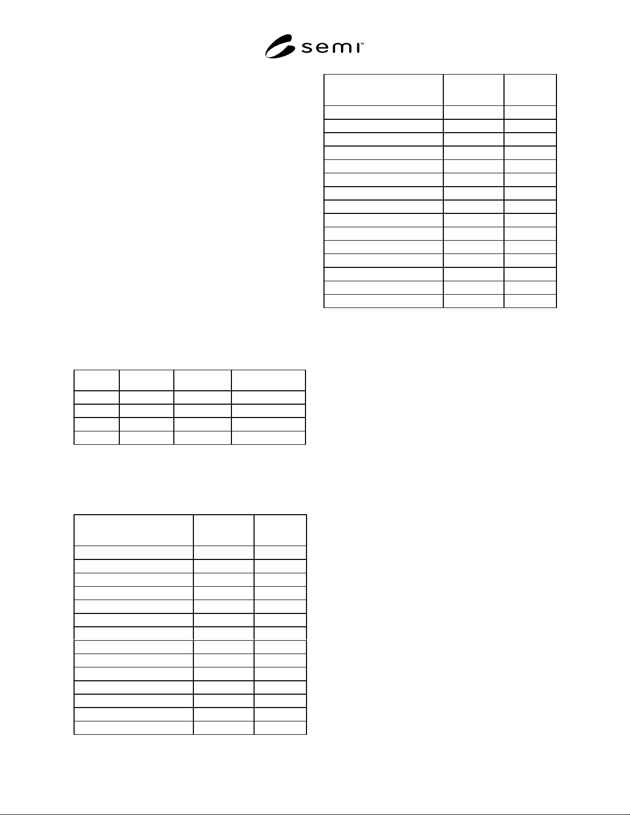
Table 2 Undercoat Finishes
Finish Copper Alloys
Nickel/Iron
Alloy
Gold MIL-G-45204
Over Base Material X
Acceptable Underplate
Nickel* X X
Silver QQ-S-365
Over Base Material X
Acceptable Underplate
Gold X
Copper X X
Tin MIL-T-10727
Over Base Material X X
Acceptable Underplate
Finish Copper Alloys
Nickel/Iron
Alloy
Nickel
XX
Copper X X
Copper MIL-C-14550
Over Base Material X X
Acceptable Underplate
Nickel QQN-290
Over Base Material X X
Acceptable Underplate
Palladium
Over Base Material
Acceptable Underplate Nickel X X
Copper X X
*Copper strike may be used under nickel.
6 Sampling
6.1 The sampling plan shall be agreed between user
and supplier.
7 Equipment
7.1 Beta Backscatter system.
7.2 Die Attach equipment.
7.3 Eutectic Die Attach heater block or hot plate
capable of 450°C ± 10°C.
7.4 Microscope 10–30× magnification with 45°
lighting.
7.5 Micro Cross-Section equipment.
7.6 Toolmaker’s Microscope
7.7 Wire Bond equipment
7.8 X-ray Fluorescence system
7.9 Solderability equipment
8 Incoming Inspection
If incoming inspection is performed, materials shall be
inspected in the following sequence:
8.1 Visual Inspection
8.2 Surface Finish
8.3 Plating Area and Thickness
8.4 Plating Quality — Heat Test a nd Adhesion Test
8.5 Functional Tests
8.5.1 Die Attach