semi合集-English.pdf - 第6108页
SEMI G21-94 © SEMI 198 0, 1996 5 NOTICE: T hese standards do n ot purport to address safety issues, if any, ass o ciated with their use. It is the responsibility of t he user of these standards to establish appropriate s…

SEMI G21-94 © SEMI 1980, 1996 4
9.5.2 Wire Bond
9.5.3 Sample leadframes shall be bonded using wire
and procedures agreed between vendor and customer.
9.5.3.1 Wires and bonds shall be tested according to
MIL-STD-883, Method 2011, and/or ASTM F 1269 by
agreement between vendor and customer.
9.5.4 Tin Plate Solderability
9.5.5 The solderability or alloying capability of the tin
plate shall be evaluated per procedures agreed between
vendor and customer.
9.6 Plating Hardness
9.6.1 Where required for verification of results
obtained in other tests, the plating hardness shall be
measured per ASTM E 384.
10 Certification
10.1 Upon request by the customer in the purchase
order, a vendor’s certification that the plating was
performed and tested in accordance with this
specification, together with a report of the test results,
shall be furnished at the time of shipment. This
certification does not remove the vendor's responsibility
for discrepant product subsequently found by the
customer.
10.2 When certification is requested, the following
information shall be supplied as a minimum
requirement:
10.2.1 Vendor Name
10.2.2 Purchase Order Number
10.2.3 Vendor Lot Number
10.2.4 Customer Part Number
10.2.5 Plating Type, Grade and Measured Thickness
for Under and Finsh Plates
10.2.6 Plating hardness if agreed between vendor and
user.
11 Packaging and Marking
11.1 Packaging
11.1.1 Shipping containers and materials shall be
suitably selected to provide the material with protection
from normal transportation damage risks which include
crushing, abrasion, spillage, and exposure to moisture
and other corrosive gases. The inner packing materials
may be further specified by the customer for cleanliness
and non-tarnishing issues.
11.2 Marking
11.2.1 Internal Packages — Each internal package
shall be marked as follows:
Vendor’s Name
Customer’s Part Number
Customer’s Order Number
Vendor’s Specification Number and Customer’s, if
appropriate
Manufacturing Lot Number
Quantity
Date of Manufacture
11.2.2 External Packages
Customer’s Specification Number
Customer’s Order Number
Quantity
Shipping Date
Any specific instructions for receiving dock
personnel if requested on the purchase order
12 Discrepancy Material
12.1 Material rejected at incoming inspection shall be
segregated and tagged as rejectable.
12.2 The vendor shall be informed and the returned
goods policy activated.
Note 7: Samples showing the defects shall be identified for
the vendor. If the vendor wishes to see the samples before
return of the complete shipment, the material shall be stored
by the customer in a manner to prevent further damage or
deterioration.

SEMI G21-94 © SEMI 1980, 19965
NOTICE: These standards do not purport to address
safety issues, if any, associated with their use. It is the
responsibility of the user of these standards to establish
appropriate safety and health practices and determine
the applicability of regulatory limitations prior to use.
SEMI makes no warranties or representations as to the
suitability of the standards set forth herein for any
particular application. The determination of the
suitability of the standard is solely the responsibility of
the user. Users are cautioned to refer to manufacturer’s
instructions, product labels, product data sheets, and
other relevant literature respecting any materials
mentioned herein. These standards are subject to
change without notice.
The user’s attention is called to the possibility that
compliance with this standard may require use of
copyrighted material or of an invention covered by
patent rights. By publication of this standard, SEMI
takes no position respecting the validity of any patent
rights or copyrights asserted in connection with any
item mentioned in this standard. Users of this standard
are expressly advised that determination of any such
patent rights or copyrights, and the risk of infringement
of such rights, are entirely their own responsibility.
Copyright by SEMI® (Semiconductor Equipment and Materials
International), 3081 Zanker Road, San Jose, CA 95134. Reproduction o
f
the contents in whole or in part is forbidden without express written
consent of SEMI.
SEMI G22-1296 © SEMI 1980, 19961
SEMI G22-1296
SPECIFICATION FOR CERAMIC PIN GRID ARRAY PACKAGES
1 Purpose
This specification defines the acceptance criteria for
cofired ceramic pin grid array packages.
2 Scope
This specification includes the visual, dimensional, and
functional requirements for the ceramics PGA package.
3 Referenced Documents
3.1 Military Standards
1
MIL-G-45204 — Gold Plating, Electrodeposited
MIL-I-23011 — Iron Nickel Alloys for Sealing to
Glasses and Ceramics
MIL-PRF-38535 — Integrated Circuits (Microcircuits)
Manufacturing, General Specification for
MIL-STD-105 — Sampling Procedures and Tables for
Inspection by Attributes
MIL-STD-883 — Test Methods and Procedures for
Microelectronics
MIL-STD-1835 — Interface Standard for Microcircuit
Case Outlines
MIL-STD-7883 — Brazing
QQ-N-290A — Nickel Plating
3.2 Other Documents
ANSI Y14.5
2
— Dimensioning and Tolerancing
JEDEC Pub. No. 95
3
— Registered and Standard
Outlines for Semiconductor Devices
4 Terminology
4.1 blister (bubble) ceramic — Any separation within
the ceramic which does not expose underlying ceramic
material.
4.2 blister (bubble) metal — Any localized separation
within the metallized or between the metallization and
ceramic which does not expose underlying metal or
ceramic material.
1 Military Standards, Naval Publications and Form Center, 5801
Tabor Ave., Philadelphia, PA 19120
2 ANSI, 1430 Broadway, New York, NY 10018
3 JEDEC, 2500 Wilson Blvd., Arlington, VA 22201-3834
4.3 braze — An alloy with a melti ng point equal to or
greater than 450°C.
4.4 burr — An adherent fragment of excess parent
material, either horizontal or vertical, adhering to the
component surface.
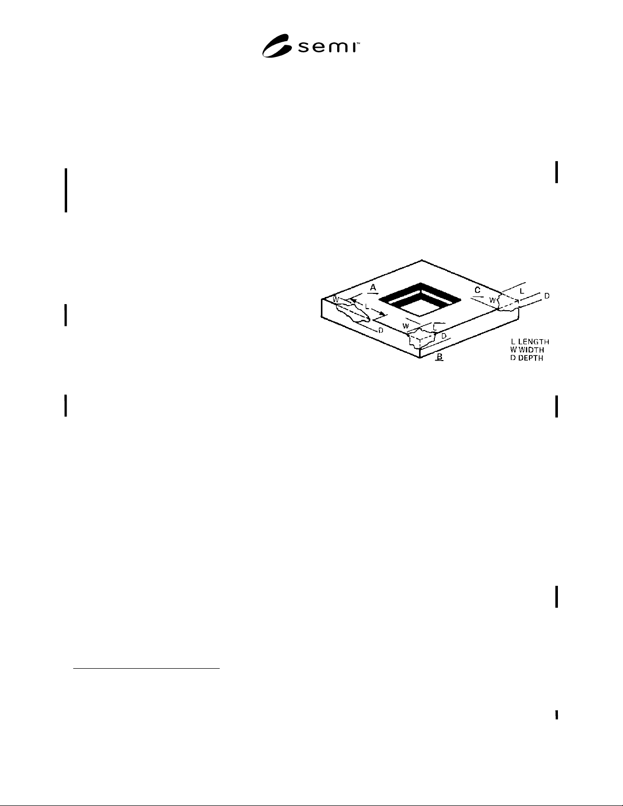
4.5 chip — A region of ceramic missing from the
surface or edge of a package which does not go
completely through the package. Chip size is given by
its length, width, and depth from a projection of design
plan form (Figure 1).
Figure 1
Chip Illustration
4.6 cofired — A process or technology for
manufacturing products in which the ceramic and
refractory metallizations are fired simultaneously.
4.7 contact pad — That metallized pattern that
provides mechanical or electrical connection to the
external circuitry.
4.8 crack — A cleavage or fracture that extends to the
surface of a package. It may or may not pass through
the entire thickness of the package.
4.9 delamination — The separation of the individual
layers of the ceramic.
4.10 die attach area — A dimensional outline
designated for die attach.
4.11 discoloration — Any change in the color of the
package plating or metallization as detected by the
unaided eye which normally appears after the
application of heat per Section 8.7.1.
4.12 flatness — The allowable deviation of a surface
from a reference plane. The tolerance zone is defined
by two parallel planes within which the surface must
lie.
4.13 footprint — Pin pattern.
4.14 foreign material — An adherent particle other
than parent material of that component.