semi合集-English.pdf - 第6187页
SEMI G39-89 © SEMI 198 6, 1989 3 8.3.3 Metallized Seal Area — 0.025 m m (0.001"), maxi mum. 8.3.4 Bottom Surface — 0.051 mm ( 0 . 002"), maxi mum. 8.3.5 Edges — 0.152 mm (0.006"), m a xi mum . 8.3.6 T ermi…

SEMI G39-89 © SEMI 1986, 1989 2
TIR — total Indicator Reading; the span of readings
from minimum to maximum of a given dimension over
the total surface to which it applies.
void (ceramic) — an absence of screen printed ceramic
from a designated area greater than 0.075 mm (0.003")
in diameter.
void (metal) — an absence of refractory metallization,
braze or plating material from a designated area greater
than 0.075 mm (0.003") in diameter.
4 Ordering Information
4.1 Purchase orders for co-fired ceramic brazed lead
flatpack packaged devices shall specify the following
information:
1. Quantity.
2. Drawing number and revision level or date.
3. Reference to this specification.
4. Any exception to drawing or specification.
4.2 Drawings for co-fired ceramic brazed lead flatpack
packaged devices shall specify the following
information:
1. Drawing number and revision level.
2. Number of terminals and terminal center line
pacing.
3. Lead material, finish, and dimensions.
4. Ceramic material color and composition; and
refractory metal type.
5. Type and thickness of plating on both device body
and leads.
6. Dimensioning and tolerancing per ANSI Y14.5.
7. Internal bonding pattern.
8. Lead number 1 position.
9. Method of test and measurements.
10.Electrical, mechanical and environmental
requirements.
5 Dimensions and Permissi ble Variations
Packaged device dimensions shall conform to JEDEC
JC-11 registered outline dimension drawings for Co-
fired Ceramic Brazed Lead Flatpack Devices for
Automated Assembly, unless otherwise specified.
6 Materials
6.1 Ceramic
6.1.1 Alumina Content — To be 90% minimum.
Beryllia content to be 99% minimum.
6.1.2 Color — To be black, dark brown, or dark violet
unless otherwise specified.
6.2 Metals — External metal surfaces shall be in
accordance with MIL-M-38510.
6.3 Braze — Copper/silver per MIL-STD-7883.
6.4 Refractory Metallization — To be per MIL-M-
38510, Type C.
6.5 Leadframe — Fully annealed iron nickel cobalt
alloy (per MIL-M-38510, Type A) or iron nickel alloy
(per MIL-M-38510, Type B).
6.6 Microcircuit Finishes — Shall be per MIL-M-
38510 unless otherwise specified.
7 Incoming Testing Sequen ce
1. Visual inspection.
2. Dimensional check.
3. Electrical parameter testing.
4. Sampling testing of plating quality, die attach, die
shear, wire bond pull, seal, hermeticity, lead
integrity, and solderability.
8 Visual Criteria (10× Magni fication)
8.1 Cracks — None allowed per MIL-STD-883,
Method 2009.
8.2 Chip-Outs
8.2.1 Corner — 0.762 mm (0.030") × 0.762 mm
(0.030") × 1 tape layer, maximum.
8.2.2 Edge — 2.54 mm (0.100") × 0.762 mm (0.030")
× 1 tape layer, maximum.
8.2.3 Encroachment — No encroachment upon seal
areas, bonding fingers, or external terminal areas
permitted. Chips that expose any buried metallization
are not permitted.
8.3 Burrs, Projections, and Blisters — Must fit within
outline limits.
8.3.1 Top Plane — excluding seal area — 0.102 mm
(0.004"), maximum.
8.3.2 Unmetallized Seal Area — 0.0762 mm (0.003"),
maximum.
SEMI G39-89 © SEMI 1986, 19893
8.3.3 Metallized Seal Area — 0.025 mm (0.001"),
maximum.
8.3.4 Bottom Surface — 0.051 mm (0.002"),
maximum.
8.3.5 Edges — 0.152 mm (0.006"), maximum.
8.3.6 Terminal Pads — 0.051 mm (0.002"),
maximum.
8.3.7 Wire Bond Fingers — 0.025 mm (0.001"),
maximum.
8.3.8 Die Attach Surface Flatness — 0.025 mm
(0.001"), maximum.
8.4 Camber — .004 inch/inch (mm/mm), maximum.
For dimensions less than 10.5 mm (0.750"), 0.127 mm
(0.003") camber is permitted along any planar
dimension of the device package.
8.5 Seal Area Flatness — The seal area shall be within
the limits listed in Table 1.
8.6 Die Attach Surface Flatness — The die attach
surface shall be flat within the limits listed in Table 2.
Table 1 Seal Ring Flatness Limits
Seal Ring O.D. Seal Ring Flatness
0—6.35 mm (0–0.250") 0.051 mm max. (0.002")
6.37—12.7 mm (0.251"–0.500") 0.051 mm max. (0.002")
12.72—25.40 mm (0.501"–
1.000")
0.101 mm max. (0.004")
25.40 mm (1.000") 0.101 mm/mm (0.004"/in.)
Table 2 Die Attach Area Flatness Limits
Die Attach Pad Dimension TIR Flatness
0—12.7 mm (0—0.500") 0.051 mm max. (0.002")
12.72—19.5 mm (0.501"—0.750") 0.088 mm max. (0.0035")
8.7 Voids
8.7.1 Seal Area Voids — A maximum of 3 voids
permitted. Not more than two voids per side of 0.010"
diameter. Any two voids must be separated by 0.762
mm (0.030") minimum, not to degrade the seal width
by more than 25%.
8.7.2 Terminal Void — A maximum of two voids per
terminal pad permissible. Maximum void diameter
acceptable is 0.254 mm (0.101). Voids may never
reduce the minimum terminal width to less than 2/3 of
the nominal design dimension.
8.7.3 Wire Bond Finger Voids — Void free 0.015"
back from the bond finger tip.
8.7.4 Die Attach Surface Voids — Three voids of
0.010" diameter are the maximum allowed separated by
0.030" minimum.
NOTE — Voids 0.015" from the cavity wall not included.
8.7.5 Internal Metallization Voids — Voids in internal
metallization planes or traces shall not break continuity.
Specific requirements for resistance and capacitance
parameters shall be specified in the purchase order, if
applicable.
8.8 Pattern Metallizations
8.8.1 Seal Plan Rundown (internal cavity) — Not to
exceed 25% of the cavity layer thickness.
8.8.2 Seal Plan Rundown (external to cavity) — Not
to exceed half the nominal design distance to adjacent
edge metallization. In no event shall the rundown be
closer than 0.254 mm (0.010") to any edge
metallization.
8.8.3 Wire Bond Rundown — Wire bond finger
rundown shall not exceed 25% of the cavity depth or
0.005" (0.127 mm) whichever is smaller.
8.8.4 Wire Bond Finger Pullback — Wire bond finger
pullback shall not exceed 0.127 mm (0.005") from the
nominal design dimension for finger end to cavity edge.
8.8.5 Seal Plane Pullback — Seal plane pullback shall
not exceed 0.127 mm (0.005") from the nominal design
dimension for seal plane metallization to edge.
8.9 Lead Attachment
8.9.1 Voids in Braze — Braze fillets must be 95% free
of voids, shall not cause voids under a lead.
8.9.2 Lead Offset — Lead centerlines must be aligned
to within 0.127 mm (0.005") of the centerlines of
corresponding braze pad metallizations. Side to side
within 0.010".
8.9.3 Lead-to-Lead Misalignment — To exceed 10%
of nominal spacing.
8.9.4 Dimensional Criteria — Per JEDEC JC-11
registered outline drawings in JEDEC Publication 95,
or as specified on the user drawings.
9 Sampling
Sample size must meet requirements of MIL-STD-105
or MIL-M-38510 as agreed to between user and
supplier.
10 Test Methods (Mechanical, Electrical, and
Thermal)
10.1 Gold Plating Thickness — Shall conform to
MIL-STD-45204. Gold thickness may be determined
SEMI G39-89 © SEMI 1986, 1989 4
using the Beta Backscatter Radiation Method, X-Ray
Fluorescence or by Cross Sectioning.
10.2 Nickel Plating — Shall conform to QQ-N-290.
Nickel thickness may be determined using the Beta
Backscatter Radiation Method, X-Ray Fluorescence, or
by Cross Sectioning.
10.3 Destructive Die Shear Testing — Shall be
performed per Method 2019 of MIL-STD-883.
10.4 Wire Bond Pull Testing — Shall be performed
per Method 2011, Condition D of MIL-STD-883.
10.5 Temperature Cycling Testing — Shall be
performed per Method 1010, Condition C of MIL-STD-
883.
10.6 Thermal Shock Testing — Shall be performed per
Method 1011, Condition C of MIL-STD-883.
10.7 Constant Acceleration Testing — Shall be
performed per Method 2001, Condition E, Y axis only,
of MIL-STD-883.
10.8 Mechanical Shock Testing — Shall be performed
per Method 2002, Condition B of MIL-STD-883.
10.9 Insulation Resistance Testing — Shall be
performed per Method 1003 of MIL-STD-883.
10.10 Internal Water Vapor Content Testing — Shall
be performed per Method 1018 of MIL-STD-883.
10.11 Hermeticity Testing — Shall be performed per
Method 1014, Condition A of MIL-STD-883. The
hermetic integrity of the packaged device must be
maintained after all testing.
10.12 Lead Integrity Testing — Shall be performed
per Method 2004, Condition A, B1, and B2 of MIL-
STD-883.
10.13 Solderability Testing — Shall be performed per
Method 2003 of MIL-STD-883.
10.14 Moisture Resistance Testing — Shall be
performed per Method 1004 of MIL-STD-883.
11 Packaging and Marking
11.1 Packaging — Containers selected shall be strong
enough and suitably designed to provide maximum
protection against crushing, spillage and other forms of
damage to the container or its contents. Container shall
afford protection of the contents to contamination from
exposure to excessive moisture or oxidation by gases.
Packaging material shall be so selected to prevent any
contamination of the ceramic component parts with
fibers or organic particles.
11.2 Marking — The outer containers shall be clearly
marked identifying:
1. Supplier part number.
2. User part number.
3. Quantity.
4. Date of manufacture.
5. Supplier lot number.
12 Applicability
This specification is intended to apply to construction
utilizing the tall brazed lead flatpack outlines included
in JEDEC Publication 95.
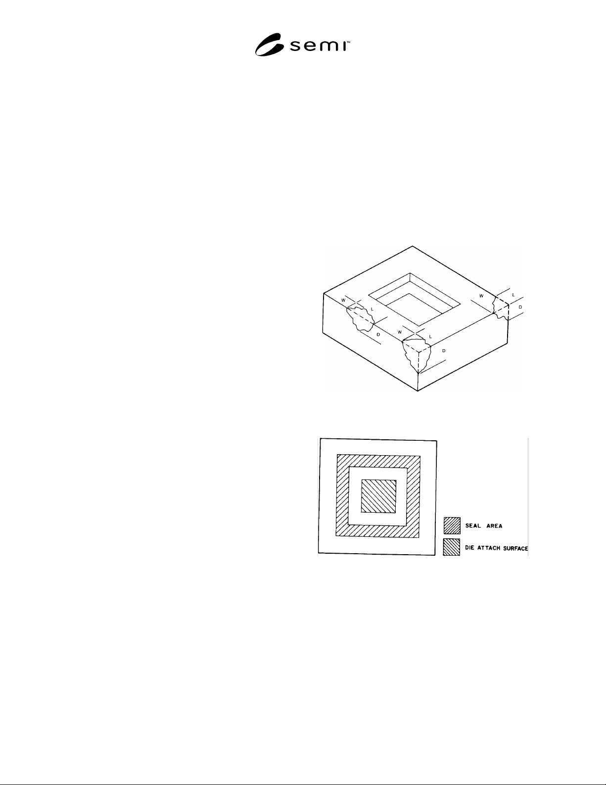
Figure 1
Chip Illustration
Figure 2
Die Attach Surface and Seal Area