semi合集-English.pdf - 第6190页
SEMI G41-87 © SEMI 1987 1 SEMI G41-87 SPECIFICA TION FOR DUAL STRIP SOIC LE A DFR A M E 1 Preface Thi s specific atio n is a guide line for high vo lu me production of leadf ra mes, in cluding internal packag e plating, …
SEMI G39-89 © SEMI 1986, 19895
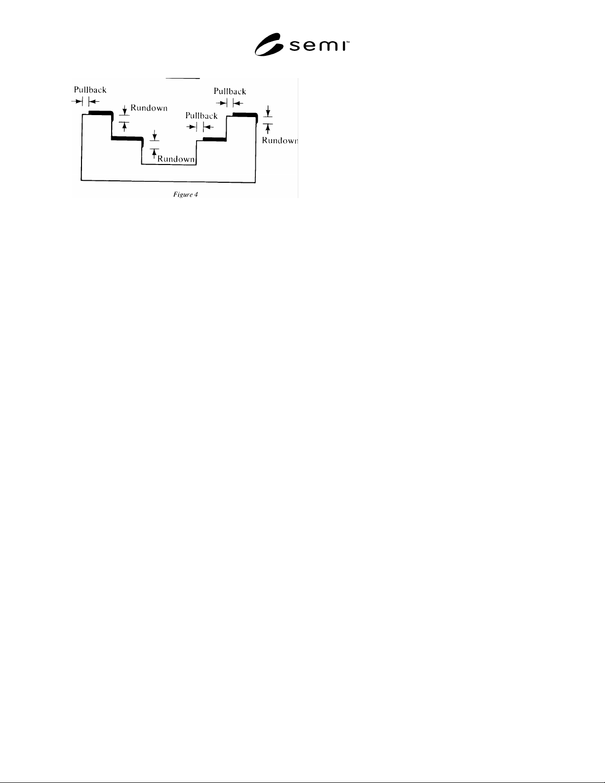
Figure 3
Metallization Misalignment
NOTICE: These standards do not purport to address
safety issues, if any, associated with their use. It is the
responsibility of the user of these standards to establish
appropriate safety and health practices and determine
the applicability of regulatory limitations prior to use.
SEMI makes no warranties or representations as to the
suitability of the standards set forth herein for any
particular application. The determination of the
suitability of the standard is solely the responsibility of
the user. Users are cautioned to refer to manufacturer’s
instructions, product labels, product data sheets, and
other relevant literature respecting any materials
mentioned herein. These standards are subject to
change without notice.
The user’s attention is called to the possibility that
compliance with this standard may require use of
copyrighted material or of an invention covered by
patent rights. By publication of this standard, SEMI
takes no position respecting the validity of any patent
rights or copyrights asserted in connection with any
item mentioned in this standard. Users of this standard
are expressly advised that determination of any such
patent rights or copyrights, and the risk of infringement
of such rights, are entirely their own responsibility.
Copyright by SEMI® (Semiconductor Equipment and Materials
International), 3081 Zanker Road, San Jose, CA 95134. Reproduction o
f
the contents in whole or in part is forbidden without express written
consent of SEMI.

SEMI G41-87 © SEMI 19871
SEMI G41-87
SPECIFICATION FOR DUAL STRIP SOIC LEADFRAME
1 Preface
This specification is a guideline for high volume
production of leadframes, including internal package
plating, for plastic molded S.O. semiconductor
packages. It is a design guideline for packaging
engineers, leadframe stampers and mold manufacturers
and has been developed to meet the requirements of
automated assembly.
2 Applicable Documents
2.1 SEMI Specifications
SEMI G4 — Integrated Circuit Leadframe Materials
used in the Production of Stamped Leadframes
SEMI G10 — Mechanical Measurement for Plastic
Package Leadframes
2.2 Military Specifications
1
MIL-STD-105 — Sampling Procedures and Tables for
Inspection by Attributes
MIL-STD-883 — Test Methods and Procedures for
Microelectronics
3 Selected Definitions
burr — a fragment of excess material either horizontal
or vertical attached to the leadframe.
camber — curvature of the leadframe strip edge (see
Figure 1).
coil set — longitudinal bowing of the leadframe (see
Figure 2).
coined area — that area at the tip end of the bond
fingers coined to produce a flattened area for wire bond
(see Figure 3).
crossbow — transverse bowing of the leadframe (see
Figure 4).
functional area — the die attach pad and the lead tips.
lead twist — angular rotation of bonding fingers (see
Figure 5).
pits — shallow surface depressions or craters in the
leadframe material.
slug marks — random dents in the leadframe caused by
foreign material in the stamping die.
1 Military Standards, Naval Publications and Form Center, 5801
Tabor Avenue, Philadelphia, PA 19120
stamped leadframe terminology — (See Figure 6.)
Z plane — lead and pad planarity require a reference in
the Z dimension. The recommendation for the reference
plane, hereafter called the Z plane, is the average of the
two dambars when measured at their geometric center.
This reference method is incorporated into SEMI G10.
4 Ordering Information
4.1 Purchase orders for leadframes for plastic molded
S.O. packages furnished to this specification shall
include the following items:
1. Part specification number and revision level
2. Material
3. Number of leads
4. Material certification
5. Packaging and marking (see Section 8)
5 Dimensions
See Table 1 and Figure 7.
6 Defect Limits and Parameters
(See SEMI G10 for Measurement Methods)
6.1 Internal Frame Area
6.1.1 Minimum Flat Wire Bonding Area — 80% of
nominal lead width and 0.381 mm (0.015") in length.
6.1.2 Coin Depth
6.1.2.1 0.20 mm (0.008") material: 0.013 mm
(0.0005") minimum/0.02 mm (0.001") maximum.
6.1.2.2 0.25 mm (0.010") material: 0.013 mm
(0.0005") minimum/0.05 mm (0.002") maximum.
NOTE: Maximum coin depth may also be constrained by
minimum lead spacing requirement given in Section 6.1.3.
Minimum coin depth may also be constrained by minimum
bond area requirement given in Section 6.1.1.
6.1.3 X-Y Plane Lead Spacing and Location
6.1.3.1 Spacing between leads to be 0.152 mm
(0.006") minimum.
6.1.3.2 Leads to be located so that a 0.007" diameter
circle centered on the nominal center of the coined lead
in width and 0.152 mm (0.006") back from lead tip in
length shall be totally encompassed by the coined area.

SEMI G41-87 © SEMI 1987 2
6.1.4 X-Y Plane Die Attach Pad Location — Die
attach pad to be located within ± 0.151 mm (0.002") as
measured from the centerline of the reference hold in
the side rail.
6.1.5 Lead Twist — Shall not exceed 330 or 0.015 mm
(0.0006") per 0.254 mm (0.010") of lead width.
6.1.6 Die Attach Pad Tilt and Flatness
6.1.6.1 Tilt — 0.025 mm (0.001") maximum per 2.54
mm (0.100") in the undepressed state. 0.051 mm
(0.002") maximum per 2.54 mm (0.100") in the
depressed condition.
6.1.6.2 Flatness — 0.0005 mm (0.0002") when
measuring from the center to the average of the four
corners. The corners are defined at 0.127 mm (0.005")
from each edge.
6.1.7 Die Attach Pad Downset — ± 0.051 mm
(0.002") as measured from the center of the pad to a
point on the bar support strip. The nominal downset
recommended is 0.30 mm (0.012") for 0.25 mm
(0.010") thick material and 0.20 mm (0.008") for 0.20
mm (0.008") thick material.
6.1.8 Lead and Die Attach Pad Coplanarity
6.1.8.1 Coplanarity — The relationship between the
leads and die attach pad is the axis relationship of these
parts to the Z plane.
6.1.8.2 Lead Planarity — The lead tips as measured in
the center of the back, uncoined surface of the lead tip
shall be located within the following tolerances of the Z
plane: Lead Planarity: ± 0.004".
6.1.8.3 Die Attach Pad Planarity — The die attach
pad when measured at the center must be within the
following tolerances of the Z plane: Pad Planarity: ±
0.003"/-0.005".
6.2 External Area and Strip
6.2.1 Material
6.2.1.1 0.20 mm (0.008") material thickness
recommended for 0.300" wide packages.
6.2.1.2 0.25 mm (0.010") material thickness
recommended for 0.300" wide packages.
6.2.1.3 Nominal thickness tolerances shall be ± 0.008
mm (0.0003").
6.2.1.4 Width Tolerance — ± 0.051 mm (0.002").
6.2.2 Coil Set — Maximum of 3.175 mm (0.125")
measured in a free standing state over strip length.
6.2.3 Crossbow — crossbow shall not exceed the
following dimensions: Maximum Crossbow ± 0.127
mm (0.005").
6.2.4 Camber — Shall not exceed 0.05 mm (0.002")
over a gauge length of 150 mm (6.00"). (See SEMI
G10, Section 8).
6.2.5 Progression — The progression over strip length
shall be within ± 0.051 mm (0.002") of nominal.
6.2.6 Burrs — Burrs shall be firmly attached and able
to withstand a probe force of 10 grams. Vertical burrs
inside the dambar shall not exceed 0.02 mm (0.001").
Vertical burrs outside the dambar and horizontal burrs
in any location shall not exceed 0.05 mm (0.002").
6.2.7 Pits and Slug Marks
6.2.7.1 Within functional area and on external leads
there shall be no slug marks. Pits shall not exceed .008
mm (0.0003") in depth and 0.013 mm (0.0005") in
largest surface dimension in these areas.
APPLICATION NOTE: There is a question regarding
the ability of material suppliers to meet this
specification. Revision of this specification is under
review.
6.2.7.2 Areas Other than 6.2.7.1 — Pits and
imperfections shall not affect leadframe strength
regardless of size and shall not exceed 0.05 mm
(0.002") in depth and 0.07 mm (0.005") in largest
surface dimension.
6.2.8 Strip Cutoff Location — Strip cutoff shall be
within ± 0.05 mm (0.002") of basic strip length.
7 Sampling
Sampling will be determined between user and supplier.
8 Packaging and Marking
8.1 Packaging — Leadframes must be packed in
containers designed and constructed to prevent damage
and/or contamination. Specific protection must be
provided against foreseeable mechanical and
environmental hazards.
8.2 Marking — The outer containers shall be clearly
marked, identifying the user stock number, user
purchase order number, drawing number, and vendor
lot number within the carton.