semi合集-English.pdf - 第6200页
SEMI G42-0996 © SEMI 1986, 2004 3 Table 2 Trace Dimens ion for BG A P ackage Boards Pad Pitch (mm) Trace Radius, R (mm) Solder Mask Opening Diameter Ø1 (mm) Hole Diameter Ø 2 (mm) Number of Pads 1.5 0.9 0.6 0.2 33 x 33 1…
SEMI G42-0996 © SEMI 1986, 2004 2
6 Requirements
6.1 General requirements regarding the materials used
for test board, the specified physical dimensions of the
test board and other necessary conditions are described
in the following paragraphs:
6.1.1 Material Requirements
6.1.1.1 The test board material should be NEMA Grade
G-10 or equivalent.
6.1.1.2 The conductor traces on the board must be
copper and the total amount of copper should not
exceed 20% of the surface area of the board.
6.1.1.3 The vias should be plated through.
6.1.1.4 External wire connections from the package
leads to edge connector leads must be made with 24-
gauge copper wire.
6.1.2 Thermal Test Board Physical Dimensions and
Layout — Five separate boards are designed for the
purpose of thermal measurements of different types of
semiconductor packages.
6.1.2.1 Physical Dimensions
6.1.2.1.1 Length — 114.3 mm ± 0.254 (4.50 inches ±
0.01)
6.1.2.1.2 Width — 76.2 mm ± 0.254 (3.00 inches ±
0.01)
6.1.2.1.3 Thickness — 1.524 – 1.651 mm ± 0.127 mm
(0.060 – 0.065 inches ± 0.005 inches)
6.1.2.2 Layout
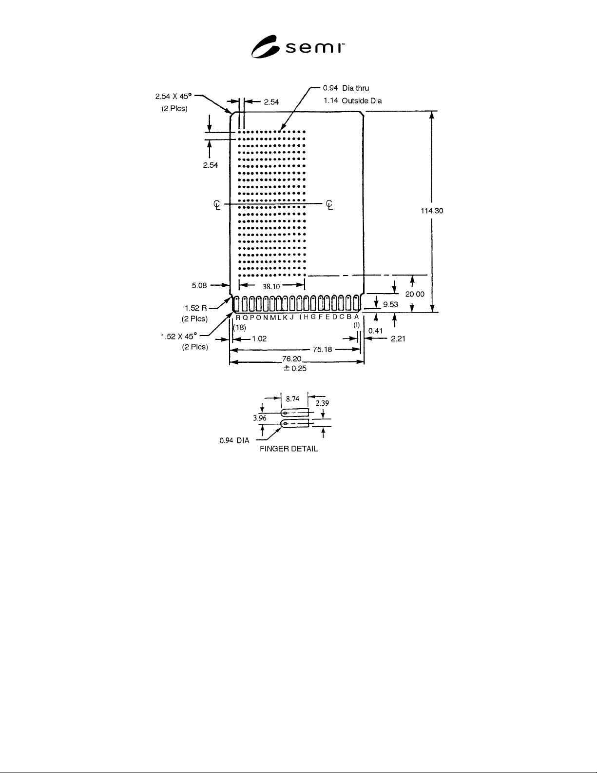
6.1.2.2.1 Dual-in-Line Packages or Sockets (See
Figure 1.)
a. The vias shall be located on 2.54 mm (0.10 inch)
centers ± 0.076 mm (0.003 inches) non-
accumulative.
b. The diameter of the vias shall be 1.143 mm (0.045
inches) ± 0.076 mm (0.003 inches).
c. The location of the vias on the board shall be as
shown in Figure 1.
6.1.2.2.2 Chip Carrier Packages (See Figure 2.)
a. The copper traces shall be laid out on the PC board
as shown in Figure 2. The traces are drawn on 1.27
mm (0.050 inch) centers ± 0.127 mm (0.005 inch)
non-accumulative.
b. The vias at the end of the copper traces shall be
located on the 2.54 mm (0.10 inch) centers ± 0.076
mm (0.003 inch) non-accumulative.
6.1.2.2.3 Quad Flat Packages (0.3, 0.4, 0.5, and 0.65
mm lead pitch) or sockets (See Figures 3–6.)
a. The copper traces shall be laid out on the PC board
as shown in Figures 3–6. The traces are drawn in
accordance with pitch and width as shown in Table
1.
Table 1 Trace Pitch and Width for QFP Package
Boards
Package Lead Pitch
(mm)
Trace Pitch (mm)
Trace Width (mm)
0.65 0.65 ± 0.05 0.35
0.5 0.5 ± 0.05 0.25
0.4 0.4 ± 0.04 0.2
0.3 0.3 ± 0.03 0.15
6.1.2.2.4 Pin Grid Array Packages or Sockets (See
Figure 7.)
a. The vias shall be located on 2.54 mm (0.10 inch)
centers ± 0.076 mm (0.003 inches) non-
accumulative.
b. The diameter of the copper lead shall be 1.2 mm ±
0.046 mm and the hole shall be 0.95 mm ± 0.046
mm.
c. The location of the vias on the board shall be as
shown in Figure 7-1.
6.1.2.2.5 Ball Grid Array Packages (1.5, 1.27, and 1.0
mm Ball Pitch) (See Figure 8.)
a. The copper traces shall be laid out on the PC board
as shown in Figure 8-1. The traces and vias are
drawn in accordance with configuration and
dimension as shown in Table 2.
b. The board shall be covered by resist as shown in
Figure 8-2. The back side of the board shall not be
covered by resist.

SEMI G42-0996 © SEMI 1986, 2004 3
Table 2 Trace Dimension for BGA Package Boards
Pad Pitch (mm)
Trace Radius, R (mm)
Solder Mask Opening
Diameter Ø1 (mm)
Hole Diameter Ø 2 (mm)
Number of Pads
1.5 0.9 0.6 0.2 33 x 33
1.27 0.8 0.6 0.35 39 x 39
1.0 0.6 0.45 0.3 49 x 49
6.1.2.2.6 Equivalent boards for other packages should
follow guidelines similar to those described in Sections
6.1.2.2.1–6.1.2.2.5.
6.1.2.2.7 Multi-Layer Board — When measuring
thermal resistance using a multi-layer board, the layer
shall be constructed as shown in Figure 9. The inner
pattern should have the clearance as shown in Figure 10
to isolate with via holes.
6.1.3 Mounting Guidelines
6.1.3.1 Example of package mounting on the boards is
shown in Figures 11 and 12. Packages should be
mounted such that the center line of the test board is
coincidental with the center line of the package.
6.1.3.2 For DIP and CCP, the longer edge of the
package should be closest to the long edge of the board.
6.1.3.3 For QFP, PGA, and BGA package board, the
package should be mounted in the center of the board.
6.1.3.4 Packages must be mounted such that the
standoff height above the board is as per JEDEC
guidelines. In the case of a new package without such
information available, a minimum of 0.127 mm (5 mil)
air gap between the bottom surface of the package and
the thermal test board is acceptable.
6.1.4 Mounting the Test Board for Still-Air R
θJA
Measurement
6.1.4.1 The test board should be mounted on a clamp
as shown in Figure 13 through a suitable edge
connector clamp.
6.1.4.2 The test board and the edge connector clamp
are placed in a 0.0283 m
3
(one cubic foot) enclosure as
shown in Figure 13. The edge connector clamp height
must be adjusted to ensure positioning of the package in
the center of the chamber.
6.1.4.3 The electrical wire connections from the
package are routed out of the one cubic foot enclosure
either through an edge connector or through small
diameter holes in the box.
6.1.5 Mounting the Test Board for Forced-Air R
θJA
Measurement — Forced air R
θJA
measurements are
performed in a wind tunnel whose diameter is 203.2
mm (8.00 inches). Details of the wind tunnel are given
in SEMI G38.
6.1.5.1 The test board should be mounted inside the
wind tunnel on an edge connector clamp as shown in
Figure 14.
6.1.5.2 The test board is placed in the wind tunnel such
that the longer edge of the package is in a vertical
position (see Figure 14).
6.1.5.3 The longer edge of the package should face the
direction of air flow.
6.1.5.4 The longer side of the package must meet the
air front first, as shown in Figure 14.
6.1.5.5 Air may be forced through the wind tunnel by
either blowing from one end or by suction. (Suction
being preferred.)
6.1.5.6 The test board and the edge connector clamp
are placed in the wind tunnel as shown in Figure 14.
The edge connector clamp height must be adjusted to
ensure positioning of the package in the center of the
wind tunnel.
6.1.6 Thermal Resistance Measurement Methods —
Methods for measuring R
θJA
(Junction-to-Ambient
Thermal Resistance) of IC packages using thermal test
chips have been described in SEMI G32 and SEMI
G38, respectively. These methods or equivalent
methods such as the use of switching techniques, as
described in MIL-STD-883C, Method 1021.1, should
be used for making thermal resistance measurements of
IC packages using thermal test chips or IC devices.
SEMI G42-0996 © SEMI 1986, 2004 4
Figure 1
Thermal Test Board — Dual In-Line Package
(Unit: mm)
1. Material — Epoxy Glass 1.52–1.65 mm thickness, FR-4 (Green). Copper Clad. 28.3 g (1 Oz.) 1/1
2. Gold-Plated Fingers — 0.8 µm Min. Thickness, 18 on Each Side
3. Fabricate — IPC-D-320, Class III
4. Tolerance — ± 0.1 mm (Unless noted)
5. Fingers on Component Side of Board — Designed as A thru R, Fingers on Solder Side of Board — Designated
as 1 thru 18 (with 18 at Right When Viewing Face of Board)
6. All Holes Plated Thru
7. Mates with Dale Connector Part Number EB 7D-A18GFX or Equivalent