semi合集-English.pdf - 第6217页
SEMI G44-94 © SEMI 198 6, 1994 1 SEMI G44-94 SPECIFICA TION FOR LE A D FINISHES FOR GLA SS TO METAL SEA L CERAMIC P A CK AGES (ACTIVE DEVICES ONLY) 1 Preface 1.1 T his specification defines lead f i nishes for glass to m…
SEMI G43-87 © SEMI 1986, 1987 4
R
ΘJR
=
T
J
−T
R
P
H(Package)
junction - to - reference point
where
R
ΘJR
= R
ΘJA
and T
R
=T
A
.
6 Summary Report
The following details shall be specified as appropriate:
a. Description of package; including thermal test chip,
location of case or chip carrier temperature
measurement(s), and mounting arrangement.
b. Test condition(s), as applicable (see Section 5).
c. Test voltage(s), current(s), and power dissipation of
test chip.
d. Recorded data for each test condition, as applicable.
e. Symbol(s) with subscript designation(s) of the
thermal characteristics determined.
f. Accept or reject criteria.
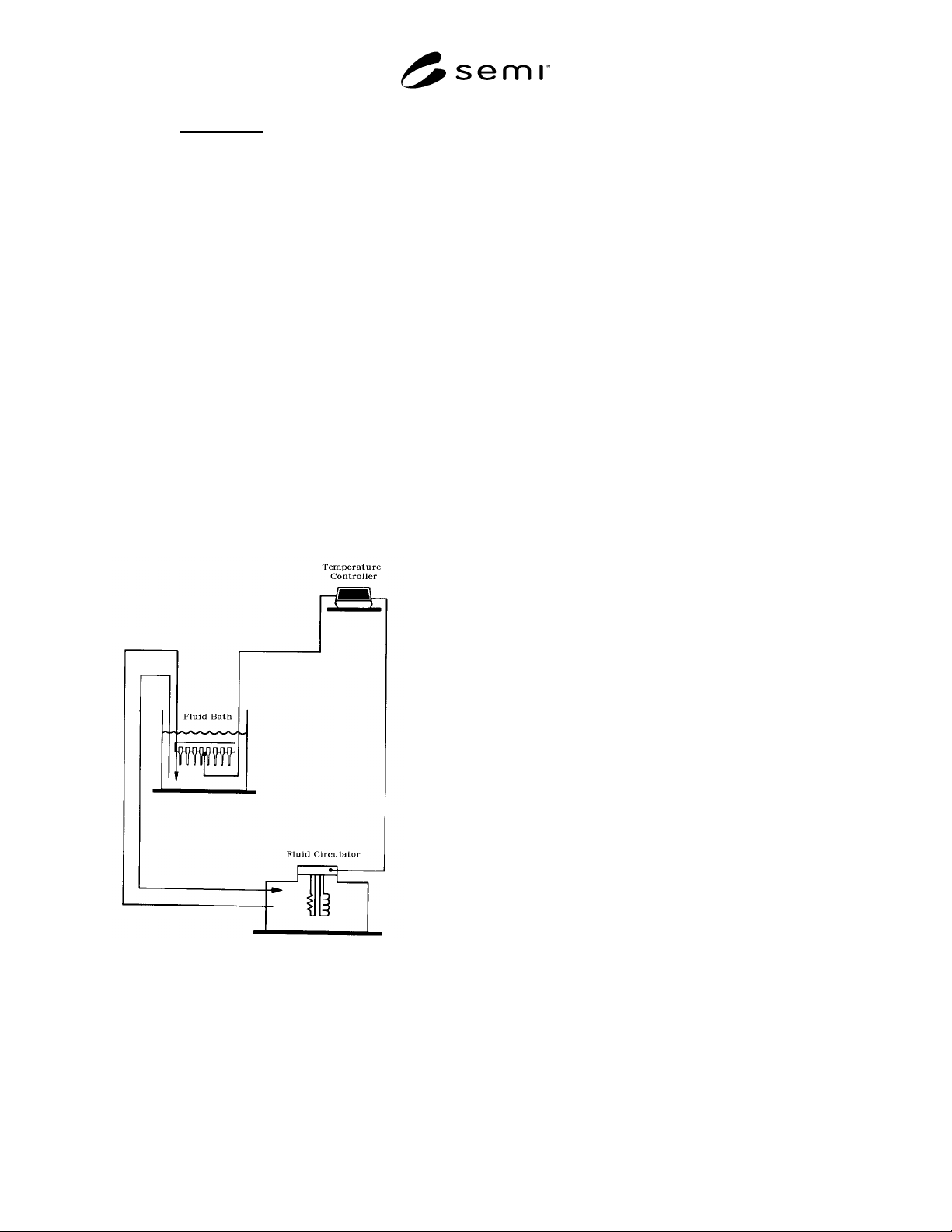
Figure 1
Temperature Controlled Fluid Bath Assembly
NOTICE: These standards do not purport to address
safety issues, if any, associated with their use. It is the
responsibility of the user of these standards to establish
appropriate safety and health practices and determine
the applicability of regulatory limitations prior to use.
SEMI makes no warranties or representations as to the
suitability of the standards set forth herein for any
particular application. The determination of the
suitability of the standard is solely the responsibility of
the user. Users are cautioned to refer to manufacturer’s
instructions, product labels, product data sheets, and
other relevant literature respecting any materials
mentioned herein. These standards are subject to
change without notice.
The user’s attention is called to the possibility that
compliance with this standard may require use of
copyrighted material or of an invention covered by
patent rights. By publication of this standard, SEMI
takes no position respecting the validity of any patent
rights or copyrights asserted in connection with any
item mentioned in this standard. Users of this standard
are expressly advised that determination of any such
patent rights or copyrights, and the risk of infringement
of such rights, are entirely their own responsibility.
Copyright by SEMI® (Semiconductor Equipment and Materials
International), 3081 Zanker Road, San Jose, CA 95134. Reproduction o
f
the contents in whole or in part is forbidden without express written
consent of SEMI.

SEMI G44-94 © SEMI 1986, 19941
SEMI G44-94
SPECIFICATION FOR LEAD FINISHES FOR GLASS TO METAL SEAL
CERAMIC PACKAGES (ACTIVE DEVICES ONLY)
1 Preface
1.1 This specification defines lead finishes for glass to
metal seal ceramic packages assembled with iron-nickel
alloy leadframe construction. It defines composition,
properties, limits, and refers to appropriate tests for
utility.
1.2 Scope — The criteria detailed in this document
applies to glass to metal seal ceramic packages,
assembled with iron-nickel alloy leadframe
construction, which conforms to composition limits
specified in MIL-M-38510 as lead material Type A or
Type B.
1.3 Units — U.S. Customary (inch -pound) or metric
(SI) units may be used at the customer’s discretion.
This specification uses U.S. Customary units as the
prime unit.
2 Applicable Documents
2.1 Order of Precedence — To avoid conflicts, the
order of precedence when ordering packages shall be as
follows:
Purchase Order
Customer Package Drawing
This Specification
Reference Documents
Related Documents
2.1.1 SEMI Specifications
SEMI G2 — Specification; Metallic Leadframes for
Cer-DIP Packages
SEMI G35 — Specification; Test Methods for Lead
Finishes on Semiconductor (Active Devices)
2.1.2 ASTM Specifications
1
B 487 — Measuring Metal and Oxide Coating
Thickness by Microscopical Examination of a Cross
Section
B 545 — Standard Specification for Electro-deposited
Coatings of Tin
B 567 — Measurement of Coating Thickness by the
Beta Backscatter Principle
1 American Society for Testing and Materials, 100 Barr Harbor
Drive, West Conshohoken, PA 19428-2959
B 568 — Measurement for Coating Thickness by X-
Ray Spectrometry
B 571 — Adhesion of Metallic Coatings
E 384 — Standard Test Methods for Micro-hardness of
Materials
2.1.3 Federal Specification
2
QQ-S-571 — Solder, Tin Alloy; Tin-Lead Alloy; and
Lead (Pb) Alloy
2.2 Military Specifications
2
MIL-T-10727 — Tin Plating; Electrodeposits or Hot
Dipped, for Ferrous and Non-Ferrous Metals
MIL-G-45204 — Gold Plating, Electrodeposited
MIL-STD-883 — Test Methods and Procedures for
Microelectronics
MIL-M-38510 — Microcircuits, General Specification
3 Terminology
blister — An enclosed localized separation of the
plating from its base metal or an underplated layer that
does not expose the underlying layer.
pit — A shallow depression or crater. The bottom of the
depression must be visible.
solder — As used in this specification, refers to tin lead
(Pb) as 63/37 or 60/40, unless otherwise specified and
agreed upon between user and supplier and stated on
procurement drawings.
4 Dimensions and Material
Composition limits, mechanical and physical
properties, dimensions and tolerances for Cer-DIP
leadframes are as stated in SEMI G2.
Table 1 lists recommended finishes for devices
employing iron nickel alloy leadframe (MIL-M-38510
Lead Material Type A or Type B).
Gold plate is useable in socketed applications as well as
in soldered applications. Hardness, grain size, and other
properties shall be specified in the procurement
drawing.
2 Military Standards, Naval Publications and Form Center, 5801
Tabor Avenue, Philadelphia, PA 19120
SEMI G44-94 © SEMI 1986, 1994 2
5 Lead Finish Requirements
5.1 Tin Electroplate
5.1.1 Composition — The tin deposit shall not be less
than 99.8% pure tin and shall not contain more than
0.05% pure carbon. The deposit is Type 1 as defined in
MIL-T-10727.
5.1.2 Characteristics — The procedure used for
evaluating the tin coating and the general requirements
for the coating shall comply with ASTM B 545 or the
latest current revision, except where noted below.
5.1.2.1 Thickness — The plated coating as measured
on the major flat of the leads shall be a minimum of 300
microinches (7.5 micrometers).
5.1.2.2 Appearance — Surface appearance shall be
smooth, fine grained, adherent and free from exposed
basis metal or underplate, visible blisters, pits, nodules,
porosity, indications of burning, excessive edge buildup
and other detrimental defects.
5.1.2.3 Hardness — None specified.
5.1.2.4 Preservation — Preservation coating, if
desired and agreed upon by user and supplier, is
acceptable. (Example: Stearic acid solution in xylol as
defined in MIL-T-10727.)
5.2 Tin Lead (SnPb) Electroplate
5.2.1 Composition — Major constituents shall be tin
and lead (Pb) with minor impurities. Range of major
constituents shall be:
Tin 50%-98%
Lead (Pb) 2%-50%
Nominal 60% Tin, 40% Lead (Pb)
NOTE: Users should be advised that many plating solutions
containing lead (Pb) also contain acid fluorides. Such
solutions will attack those glass materials commonly used in
ceramic packages. Adequate process controls must be
developed and used in conjunction with this plating process to
ensure package and device integrity.
5.2.2 Purity and Application — Per MIL-M-38510.
5.2.3 Thickness — Shall be a minimum of 7.5
micrometers (300 microinches) as measured on the
major flat of the leads.
5.2.4 Appearance — Surface appearance shall be
smooth, fine-grained, adherent, and free from exposed
basis metal or underplate, visible blisters, pits, nodules,
porosity, indications of burning, excessive edge buildup
and other detrimental defects.
5.2.5 Hardness — None specified.
5.3 Tin/Lead (Pb) Solder-Dip
5.3.1 Solder Pot Composition and Purity — Sn60 or
Sn63, per QQ-S-571.
5.3.2 Thickness — Shall be a minimum of 5
micrometers (200 microinches) as measured on the
major flat of the leads.
5.3.3 Process Conformance — Solder coating is
applicable as shown in Table 1. In addition, the coating
is acceptable as follows:
1. Over the electroplated tin or tin/lead as per Section
4.1 or 4.2.
2. Over the electroplated gold as per Section 4.4.
5.3.4 Appearance — Surface shall be smooth and
continuous.
5.3.5 Hardness — None specified.
5.3.6 Coverage — Electroplated packages.
5.3.6.1 The solder dip shall extend up to and beyond
the effective seating plane for Cer-DIPs.
5.3.6.2 The solder dip shall extend within .030" from
glass seal for Cer-Packs.
5.3.7 Coverage — Non-coated packages.
5.3.7.1 When applied over the base metal, hot solder
dip shall cover the entire lead to the glass seal or point
of emergence of the lead or metallized contact through
the package wall.
5.4 Gold Electroplate
5.4.1 Composition — Gold plating shall be applied in
accordance with MIL-G-45204 in any and all of the
following grades depending on application.
Type I 99.7% minimum
Type II 99.0% minimum
Type III 99.9% minimum
NOTE: Type II is suitable for socketing application only.
5.4.2 Thickness — Shall be 1.27–5.72 micrometers
(50-225 microinches) as measured on the major flat of
the leads per MIL-M-38510.
5.4.3 Appearance — Surface appearance shall be
smooth, fine-grained, adherent and free from exposed
basis metal or underplate, visible blisters, pits, nodules,
porosity, indications of burning, excessive edge
buildup, and other detrimental defects.
5.4.4 Purity — Composition limits are as specified in
Section 4.4.1 above. Individual metallics in the deposit
shall not exceed 0.1%. Metallic hardening agents,