semi合集-English.pdf - 第6228页
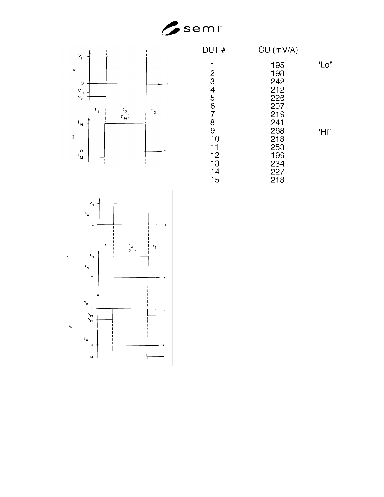
SEMI G46-88 © SEMI 1988 5 Figure 2A Waferforms Associated with Figure 1A Figure 2B Waferforms Associated with Figure 2B Figure 3 Data Results for In itial 15-Piece Sample for tH Value of 200 m s
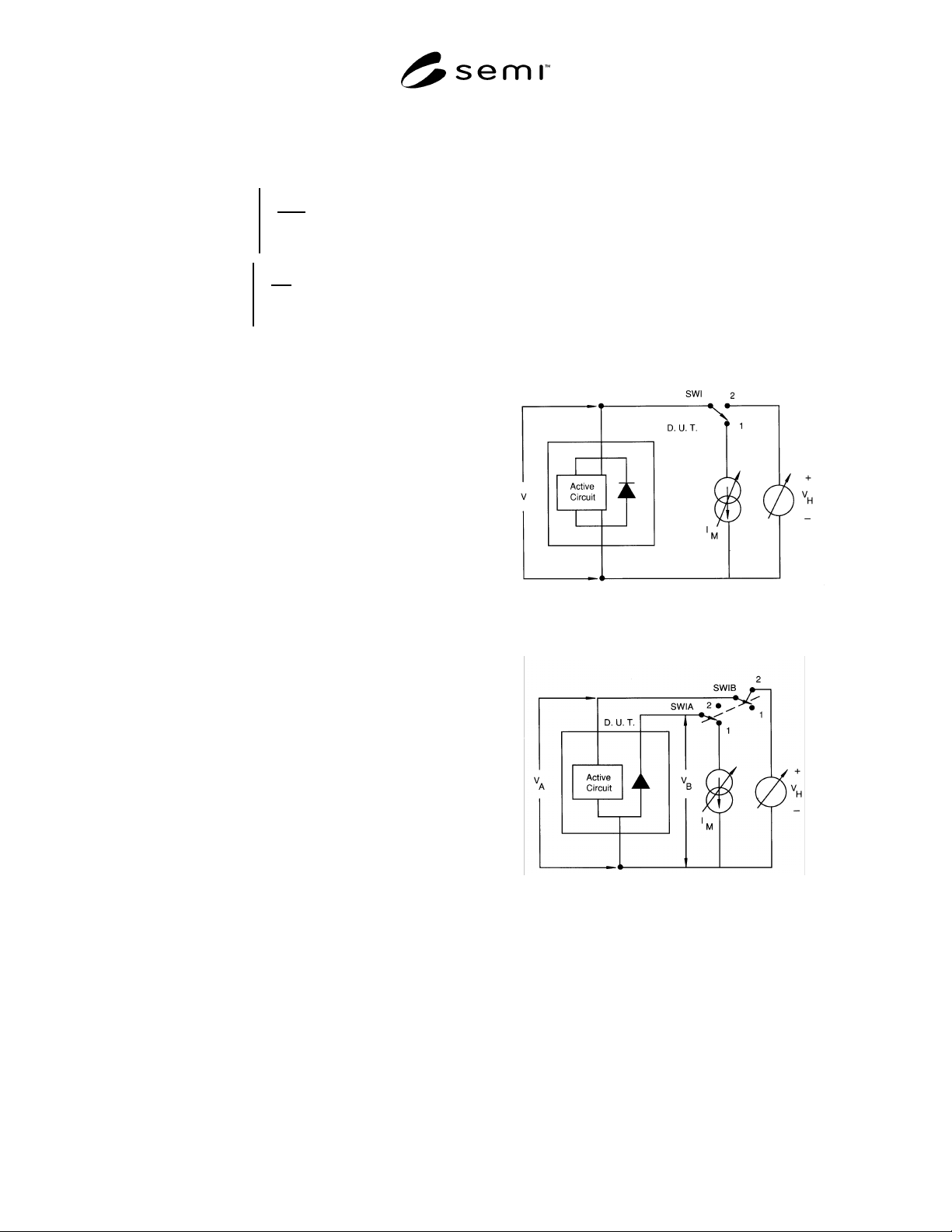
SEMI G46-88 © SEMI 1988 4
The usual rule of thumb in setting the maximum limit
for ∆V
F
or CU is to use the distribution average value
and one standard deviation ( σ) i.e. —
(∆V
F
)
high
limit
=∆V
F
+ X
σ
∆
(CU)
high
limit
= CU + X
σ
CU
Where X = 1 in most cases.
The statistical data required is obtained by testing 40 or
more devices under the conditions of Step 11.
Step 13 — Once the test conditions and pass/fail limit
have been determined, it is necessary only to record this
information for future testing requirements of the same
device in the same package. With the apparatus
properly set-up, including the fail limit selector on
those apparatus set ups so equipped, the operator need
only insert the device, initiate a test, and then either
read the ∆V
F
or CU display or observe the appropriate
pass or fail indicaors.
The steps listed hereto have been conveniently
summarized in Figure 9. The total time required to
perform these steps is greatly dependent on the operator
but, in general, should require about one hour if the
statistical approach of Step 12.C is used.
4.2
Routine Device Testing Proced ure — Once the
proper control settings have been determined for a
particular device type from a given manufacturing
process or vendor, repeated testing of that device type
simply requires that the same test conditions be used as
previously determined.
New device types or the same devices manufactured
with a different process will require a repeat of Section
4.1.
4.3
Comparison of Different Vend or Devices — Each
device type is defined as a specific chip manufactured
to a given set of procedures. Integrated circuit users
who buy a specific part number from more than one
vendor or manufacturers that redesign or otherwise
modify the fabrication of their devices will be able to
use the heating power and approximately the same t
H
for all vendors, but probably will have to use a different
∆V
F
or CU pass/fail limit for each different vendor
because the K Factor for parts manufactured by
different vendors will probably be different. The
difference can be determined in Step 12.B and using the
setup described in Figure 7.
5 Test Condition Specification
To properly set up the test apparatus and to insure
repeatable measurements, the following test conditions
must be fully specified:
a. V
H
b. t
H
c. I
M
d. t
MD
(and t
SW
if appropriate)
e. DUT/apparatus interface (i.e., wiring connection)
f. ∆V
H
or CU data requirement
Figure 1A
Set-Up for Junction Isolation Diode Devices
Figure 1B
Set-Up for Parisitic Diode or Thermal Test Chip
Temperature Sensing
SEMI G46-88 © SEMI 19885
Figure 2A
Waferforms Associated with Figure 1A
Figure 2B
Waferforms Associated with Figure 2B
Figure 3
Data Results for Initial 15-Piece Sample for tH
Value of 200 ms
SEMI G46-88 © SEMI 1988 6
Heating Time t
H
(seconds)
DUT #1 CU
(m V/A)
DUT#9 CU
(m V/A)
1 × 10
-4
43 43
1.5 43 43
24343
34343
44343
64343
84343
1 × 10
-3
45 45
1.5 45 45
24747
34848
45050
65153
85863
1 × 10
-2
63 70
1.5 75 86
2 85 100
3 100 122
4 112 140
6 130 168
8 145 190
1 × 10
-1
157 208
1.5 179 243
2 195 268
3 220 308
4 239 337
6 265 373
8 285 398
1 × 10
0
300 416
1.5 323 449
2 340 470
3 362 497
4 377 518
6 398 518
8 411 563
1 × 10
1
421 578
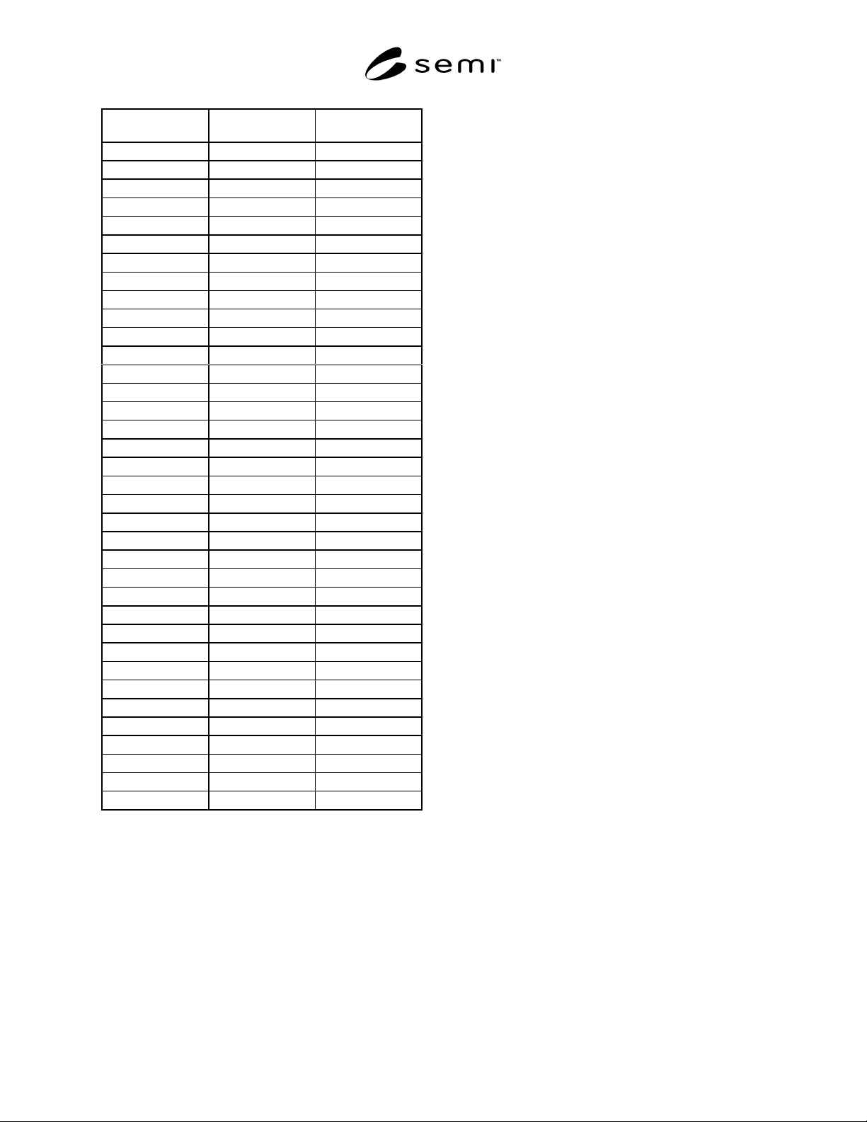
Figure 4
Heating Curve Data for Highest and Lowest Reading Devices from Figure 3