semi合集-English.pdf - 第6259页
SEMI G51-90 © SEMI 1990 1 SEMI G51-90 SPECIFICA TION FOR PLASTIC MOLDED (METRIC) QUA D FLAT PACK LEADFRAMES 1 Preface This specification defines the acceptance criteria for leadfram e s design ed for assembly of JED EC p…

SEMI G50-89 © SEMI 1989 4
10.3 Destructive Die Shear Testing — Shall be
performed per Method 2019 of MIL-STD-883.
10.4 Wire Bond Pill Testing — Shall be performed per
Method 2011, Condition D of MIL-STD-883.
10.5 Temperature Cycling Testing — Shall be
performed per Method 1010, Condition C of MIL-STD-
883.
10.6 Thermal Shock Testing — Shall be performed per
Method 1011, Condition C of MIL-STD-883.
10.7 Constant Acceleration Testing — Shall be
performed per Method 2001, Condition E, Y axis only,
of MIL-STD-883.
10.8 Mechanical Shock Testing — Shall be performed
per Method 2002 of MIL-STD-883.
10.9 Insulation Resistance Testing — Shall be
performed per Method 2002 of MIL-STD-883.
10.10 Internal Water Vapor Content Testing — Shall
be performed per Method 1018 of MIL-STD-883.
10.11 Hermeticity Testing — Shall be performed per
Method 1014, Condition A of MIL-STD-883. The
hermetic integrity of the packaged device must be
maintained after all testing.
10.12 Lead Integrity Testing — Shall be performed
per Method 2004, Condition A, B1, and B2 of MIL-
STD-883.
10.13 Solderability Testing — Shall be performed per
Method 2003 of MIL-STD-883.
10.14 Moisture Resistance — Shall be performed per
Method 2003 of MIL-STD-883.
11 Packaging and Marking
11.1 Packing — Containers selected shall be strong
enough and suitably designed to provide maximum
protection against crushing, spillage, and other forms of
damage to the container or its contents. Containers shall
afford protection of the contents to contamination from
exposure to excessive moisture or oxidation by gases.
Packaging materials shall be so selected to prevent any
contamination of the ceramic component part with
paper fibers or organic particles.
11.2 Marking — The outer containers shall be clearly
marked identifying:
1. Vendor part number
2. Customer part number
3. Quantity
4. Date of manufacture
5. Vendor lot number
12 Applicability
This specification is intended to apply to packages
fabricated to the outline requirements for the fine pitch
leaded and leadless chip carriers included in JEDEC
Publication 95.
NOTICE: These standards do not purport to address
safety issues, if any, associated with their use. It is the
responsibility of the user of these standards to establish
appropriate safety and health practices and determine
the applicability of regulatory limitations prior to use.
SEMI makes no warranties or representations as to the
suitability of the standards set forth herein for any
particular application. The determination of the
suitability of the standard is solely the responsibility of
the user. Users are cautioned to refer to manufacturer’s
instructions, product labels, product data sheets, and
other relevant literature respecting any materials
mentioned herein. These standards are subject to
change without notice.
The user’s attention is called to the possibility that
compliance with this standard may require use of
copyrighted material or of an invention covered by
patent rights. By publication of this standard, SEMI
takes no position respecting the validity of any patent
rights or copyrights asserted in connection with any
item mentioned in this standard. Users of this standard
are expressly advised that determination of any such
patent rights or copyrights, and the risk of infringement
of such rights, are entirely their own responsibility.
Copyright by SEMI® (Semiconductor Equipment and Materials
International), 3081 Zanker Road, San Jose, CA 95134. Reproduction o
f
the contents in whole or in part is forbidden without express written
consent of SEMI.
SEMI G51-90 © SEMI 19901
SEMI G51-90
SPECIFICATION FOR PLASTIC MOLDED (METRIC) QUAD FLAT PACK
LEADFRAMES
1 Preface
This specification defines the acceptance criteria for
leadframes designed for assembly of JEDEC proposed
registered Publication 95 Standard Outlines for the
Metric Quad Flat Pack Family Packages. It is a design
guideline for packaging engineers, leadframe stampers
and etchers, and mold and trim/form tooling
manufacturers. It has been developed to meet the
requirements of assemblers using automatic and manual
equipment.
2 Applicable Documents
2.1 Order of Precedence — To avoid conflicts, the
order of precedence when ordering tooling shall be as
follows:
Purchase Order
This Specification
Referenced Documents
2.2 Reference Documents
2.2.1 SEMI Specifications
SEMI G4 — Specification for Integrated Circuit
Leadframe Materials Used in the Production of
Stamped Frames
SEMI G10 — Standard Method Mechanical
Measurement for Plastic Package Leadframes
SEMI G18 — Specification for Integrated Circuit
Leadframe Material Used in the Production of Etched
Frames
SEMI G21 — Specification, Plating Integrated Circuit
Leadframes
2.2.2 ANSI Specification
1
S Y 14.5 M-1982 — Dimensioning and Tolerancing
2.2.3 JEDEC Specification
2
Reg.Prop. 11-286 — Metric Quad Flat Pack Family
(Gullwing)
1 ANSI, 1430 Broadway, New York, NY 10018
2 JEDEC, 2001 Eye Street N.W., Washington, D.C. 20006
2.2.4 Military Specification
3
MIL-STD-105 — Sampling Procedures and Tables for
Inspection by Attributes
3 Selected Definitions
burr — a fragment of excess material either horizontal
or vertical attached to the leadframe.
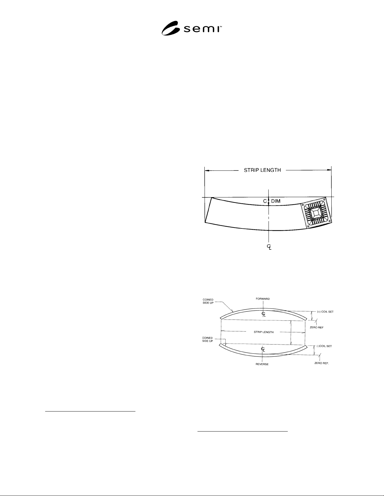
camber — curvature of the leadframe strip edge (see
Figure 1).
Figure 1
Camber
coil set — longitudinal bowing of the leadframe (see
Figure 2).
Figure 2
Coil Set
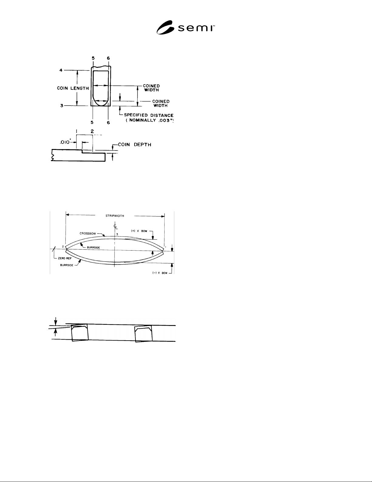
coined area — that area at the tip end of the bond
fingers coined to produce a flattened area for functional
use (see Figure 3).
3 Military Standards, Naval Publications and Form Center, 5801
Tabor Avenue, Philadelphia, PA 19120
SEMI G51-90 © SEMI 1990 2
Figure 3
Coined Area
crossbow — Transverse bowing of the leadframe (see
Figure 4).
Figure 4
Crossbow
lead twist — Angular rotation of bonding fingers (see
Figure 5).
Figure 5
Lead Twist
pits — Shallow surface depressions or craters in the
leadframe material.
true position circle — That circle with its center
positioned at the center of the coined lead defines the
design position of the lead tip.
4 Ordering Information
Purchasing orders for leadframes for plastic Molded
Quad Flat Pack packages furnished to this specification
shall include the following items:
4.1 Drawing number and revision level.
4.2 Material alloy specification.
4.3 Lead count, and confirming number of units per
strip.
4.4 Requirement for material certification.
4.5 Leadframe plating specifications.
5 Dimensions
5.1 Tables I, II.
5.2 See Figure 6 and Detail A.
6 Defect Limits and Parameters
(To measure, see SEMI G10).
6.1 Lead Tip Width
6.1.1 Minimum Lead Tip Width — Shall be as agreed
to between supplier and purchaser.
6.1.2 Minimum Flat Wire Bonding Area — 80% of
nominal lead width and 0.635 mm (0.025") in length.
NOTE: This applies to stamped frames; percent of nominal
lead width for etched frames must be determined between
purchaser and supplier and is dependent on etch tolerances.
6.2 Coining and Metal Clearance
6.2.1 If coined, maximum depth = 30% material
thickness. Minimum depth as agreed to between
supplier and purchaser.
6.2.2 On stamped frames, dimensions shown on
drawings are before coining.
6.2.3 Metal-to-Metal Clearance — Shall be as agreed
to between supplier and purchaser.
6.3 Lead Twist — Shall not exceed 3.5 or 0.015 mm
(0.0006") per 0.254 mm (0.010") of lead width.
6.4 Burrs — Shall be firmly attached and able to
withstand a probe force of 10 grams. All burrs vertical
and horizontal in any location shall not exceed 0.0254
mm (0.001").
6.5 Die Pad Tilt and Flatness — (See specification
SEMI G10 for measurement method).
6.5.1 Tilt — 0.025 mm (0.001") maximum per 2.54
mm (0.100") of length or width in the undepressed
state, and 0.051 mm (0.002") maximum per 4.06 mm
(0.160") of length or width in the depressed state, when