semi合集-English.pdf - 第6305页
SEMI G61-94 © SEMI 1994 5 6.4.1.2 St ud — (Brazed to a metallize d ar ea of the ceramic bas e layer or th e hea tsink of the packag e) — copper, tungs te n-copper, or kovar as speci fied on t he package drawing . 6.4.2 H…

SEMI G61-94 © SEMI 1994 4
3.40 side-to-side misalignment — the offset of the
center lines of corresponding leads or pins from one
side of the package to another side.
3.41 stand-off — the separation bet ween the base
plane and the seating plane that is created by physical
features that are usually formed into the pins or leads
(see Figure 6). The features may also be called stand-
offs.
3.42 TIR — total Indicator Reading.
4 Ordering Information
Purchase orders for packages furnished to this
specification shall include the following items.
4.1 Current Drawing Revision Detailing
4.1.1 All dimensions and tolerances per ANSI
Y14.5M practices.
4.1.2 Internal metallization trace pattern.
4.1.3 Type and color of ceramic.
4.1.4 Pin or Lead Material and Hardness — If
applicable.
4.1.5 Heat Sink/Stud Material and Hardness — If
applicable.
4.1.6 Type, hardness, and thickness of plating in the
die and wire bond areas and contact pads.
4.1.7 Type, Hardness, and Thickness of Plating on
Pins or Leads and Heat Sink/Stud — If applicable.
4.1.8 Lead Number 1 Identification — (See Figure 7.)
4.2 Vendor certification requirements.
4.3 Reference to this specification.
4.4 Any additions to, or variations from, this
specification.
4.5 Quantity.
5 Dimensions
Package dimensions and lead numbering shall conform
to the outlines registered with or specified by JEDEC
(see Publication 95), EIAJ or MIL-STD-1835, as
appropriate. Package manufacturing tolerances shall be
agreed between user and supplier.
6 Materials
The definitions, defect criteria, and functional tests
described in this specification relate to packages made
with the following materials.
6.1 Ceramic Body
6.1.1 Material — Alumina, beryllia, aluminum nitride,
or mullite as specified on the package drawing.
6.1.1.1 Alumina — Content to be 90% minimum.
6.1.1.2 Beryllia — Content to be 99% minimum.
(Packages shall be marked BeO.)
6.1.1.3 Aluminum nitride — Content t o be agreed
between user and supplier.
6.1.1.4 Mullite — Content to be agree d between user
and supplier.
6.1.2 Color
6.1.2.1 Alumina — White, black, dark brown, or
violet.
6.1.2.2 Beryllia — White.
6.1.2.3 Aluminum Nitride — White, black, dark
brown, or violet.
6.1.2.4 Mullite — White, black, dark brown, or violet.
6.2 Die Attach Pad, Wire Bond Fingers, Contact Pads,
and Circuit Trace Metallization
6.2.1 Base Material — Refractory tungsten per MIL-
M-38510, Type C. Thickness shall be 0.0003" (0.0076
mm) minimum.
6.2.2 Finish — Shall meet the requirements of MIL-
M-38510.
6.2.2.1 Nickel Under Plate (if specified) — Shall be
per QQ-N-290A. Thickness shall be 50 – 350 micro-
inches (0.0013 – 0.0089 mm).
6.2.2.2 Gold Plate — Shall be per MI L-G-45204,
Type III. Thickness shall be 50 – 225 micro-inches
(0.0013 – 0.005715 mm).
6.3 Pins, Leads, and Seal Ring
6.3.1 Base Material — Iron-nickel-cobalt alloy per
MIL-M-38150, Type A or iron-nickel alloy per MIL-
M-38150, Type B shall be specified on the package
drawing.
6.3.2 Hardness — 70–85 Rockwell-B for Type A
material, 60–80 Rockwell-B for Type B material.
6.3.3 Finish — Shall meet the requirements of MIL-
M-38510 per Section 6.2.2.
6.4 Heat Sink/Stud
6.4.1 Material
6.4.1.1 Heat Sink — (Forming at least part of the
package base and the die attach area) tungsten-copper
(composition to be defined on the drawing), iron-nickel
(cobalt) alloy per Section 6.3.1 or molybdenum as
specified on the package drawing.
SEMI G61-94 © SEMI 19945
6.4.1.2 Stud — (Brazed to a metallize d area of the
ceramic base layer or the heatsink of the package) —
copper, tungsten-copper, or kovar as specified on the
package drawing.
6.4.2 Hardness — Shall be specified on the drawing
by agreement between user and supplier.
6.4.3 Finish — Shall meet the requirements of MIL-
M-38510 per Section 6.2.2.
6.5 Braze
6.5.1 Material — Silver/copper (72%/28%) or
equivalent shall meet the general requirements of MIL-
STD-7883.
6.5.2 Finish — Shall meet the requirements of MIL-
M-38510 per Section 6.2.2.
7 Defect Limits
Inspection shall be carried out at 10× magnification
with vertical lighting.
The following conditions are cause for rejection.
7.1 Ceramic Components
7.1.1 Cracks — Any crack is cause for rejection.
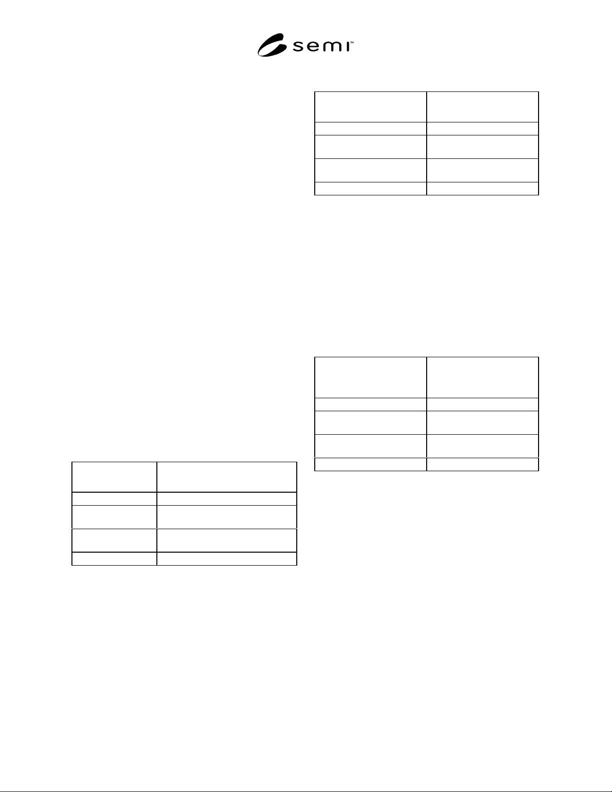
7.1.2 Chips — See Figure 3.
7.1.2.1 Corner Chips — Chip sizes ex ceeding the
limits shown in Table 1. No chip may be deeper than
50% of the package element (the ceramic functional
layer) thickness.
Table 1
Package Dimension
inch (mm)
Maximum Corner Chip Dimensions
(either direction) inch (mm)
≤0.250 (≤6.35) 0.020 (0.508)
>0.250 – ≤0.500
(>6.35 – ≤12.7)
0.040 (1.016)
>0.500 – ≤1.000
(>12.7 – ≤25.4)
0.080 (2.032)
>1.000 (>25.4) 0.100 (2.54)
7.1.2.2 Edge Chips — Chip sizes exceeding the limits
shown in Table 2. No chip may be deeper than 50% of
the package element (the ceramic functional layer)
thickness.
Table 2
Package Dimension in which
Chip Occurs inch (mm)
Maximum Chip Length and
Width inch (mm)
≤0.250 (≤6.35) 0.020 (0.508)
>0.250 – ≤0.500
(>6.35 – ≤12.7)
0.040 (1.016)
>0.500 – ≤1.000
(>12.7 – ≤25.4)
0.080 (2.032)
>1.000 (>25.4) 0.100 (2.54)
7.1.2.3 Chips exposing a buried metallized area
excluding the plating buses which are exposed when
packages are separated from the manufacturing arrays.
7.1.2.4 Critical Seal Area (ceramic) — Any chip
reducing the critical seal path length, at any point, by
more than 30% of the nominal design dimension.
No more than three chips, each of which reduces the
seal path length by more than 10% but less than 30%,
are allowed in this area. Each chip’s length shall not
exceed the limits shown in Table 3.
Table 3
Seal Ring Dimension in
which Chip Occurs
inch (mm)
Maximum Chip Length
inch (mm)
≤0.250 (≤6.35) 0.020 (0.508)
>0.250 – ≤0.500
(>6.35 – ≤12.7)
0.040 (1.016)
>0.500 – ≤1.000
(>12.7 – ≤25.4)
0.080 (2.032)
>1.000 (>25.4) 0.100 (2.54)
7.1.3 Ceramic Projections — (bumps and blisters)
7.1.3.1 Body (non-critical surfaces) — Any
projection, including fins, exceeding 0.005" (0.127
mm) in height, or exceeding 0.002" (0.051 mm) in
height and with a surface dimension greater than 0.010"
(0.254 mm).
NOTE 2: On surface mount packages, the bottom of the
package shall not have any projections exceeding 0.002"
(0.051 mm) in height.
7.1.3.2 Die Attach Areas — (bare cera mic or screen
printed metal area) — Excluding a zone, 0.015" (0.381
mm) wide, around the periphery of the cavity, any
projection exceeding 0.001" (0.025 mm) in height or a
surface dimension of 0.010" (0.254 mm).
NOTE 3: Exclusion zones around the periphery of die attach
areas may be wider on larger packages or when a metal heat
sink or stud is brazed to the package and forms the die attach
area (Section 7.3). The width of such zones shall be defined
on the package drawing by agreement between user and
SEMI G61-94 © SEMI 1994 6
supplier. This note applies to all criteria affecting die attach
areas.
7.1.3.3 Critical Seal Area (printed metal area) — Any
projection exceeding 0.001" (0.025 mm) in height or
with a surface dimension exceeding 0.010" (0.254 mm)
or 30% of the critical seal length, whichever is the
larger.
7.1.3.4 Critical Seal Area (bare ceramic) — Any
projection exceeding 0.001" (0.025 mm) in height or
with a surface dimension exceeding 0.010" (0.254 mm)
or 30% of the critical seal path, whichever is the larger.
7.1.3.5 Wire Bond Fingers — Any projection in the
critical area defined in Figure 8 exceeding 0.0005"
(0.0127 mm) in height or a surface dimension of 0.004"
(0.102 mm).
7.1.3.6 Solder Pads, Contact Pads, and Heat
Exchange Areas — Any projection exceeding 0.002"
(0.051 mm) in height above the pad, or a surface
dimension of 0.010" (0.254 mm).
NOTE 4: Castellation areas of chip carriers are excluded from
these criteria because of the manufacturing process. (Layer
misalignments, separation techniques, etc. may cause
projections which do not affect package quality.
7.1.4 Pits
7.1.4.1 Body (non-critical surfaces) — Pits exceeding
0.003" (0.076 mm) in depth or a surface dimension of
0.020" (0.508 mm).
7.1.4.2 Die Attach Areas (bare ceramic or screen
printed metal area) — Excluding a zone, 0.015" (0.381
mm) wide, around the periphery of the cavity, pits
exceeding 0.001" (0.025 mm) depth below the surface
or a surface dimension of 0.010" (0.254 mm).
Acceptable pits shall not cover more than 10% of the
surface area.
NOTE 5: Ceramic pits in metallized areas may be covered by
metallization, but remain cause for rejection.
NOTE 6: Pits with a depth not exceeding 0.0005" (0.0127
mm) are not rejectable.
7.1.4.3 Critical Seal Area (bare ceramic or metallized
area) — Pits exceeding 0.001" (.025 mm) depth below
the ceramic surface or a surface dimension of 0.010"
(0.254 mm). No more than three acceptable pits
allowed in this area with a minimum separation of
0.030" (0.762 mm) required between sites. The seal
ring width must not be reduced by more than 30% of its
designed width at any point. Acceptable pits shall not
cover more than 10% of the critical seal area.
7.1.4.4 Wire Bond Fingers — Any pit in the critical
area defined in Figure 8 exceeding 0.0005" (0.0127
mm) in depth, or any pit exeeding 0.004" (0.102 mm) in
a surface dimension.
7.1.4.5 Solder Pads, Contact Pads, and Heat
Exchange Areas — Pits exceeding 0.002" (0.051 mm)
depth below the pad or a surface dimension of 0.010"
(0.254 mm). Acceptable pits shall not cover more than
10% of the surface area.
NOTE 7: Pits with a depth not exceeding 0.0005" (0.0127
mm) are not included in this evaluation, regardless of surface
dimension.
NOTE 8: Pits in castellation areas are exluded from these
criteria because of the manufacturing process.
7.1.5 Flatness (Camber)
7.1.5.1 Package Flatness — Flatness variation
exceeding 0.004 inch/inch (0.004 mm/mm), with a
minimum camber specification of 0.002" (0.051 mm).
7.1.5.2 Die Attach Area Flatness — Any flatness
variations exceeding the limits shown in Table 4.
NOTE 9: These criteria apply to any die attach area ceramic,
metallized ceramic, or a heat sink which forms the die attach
area.
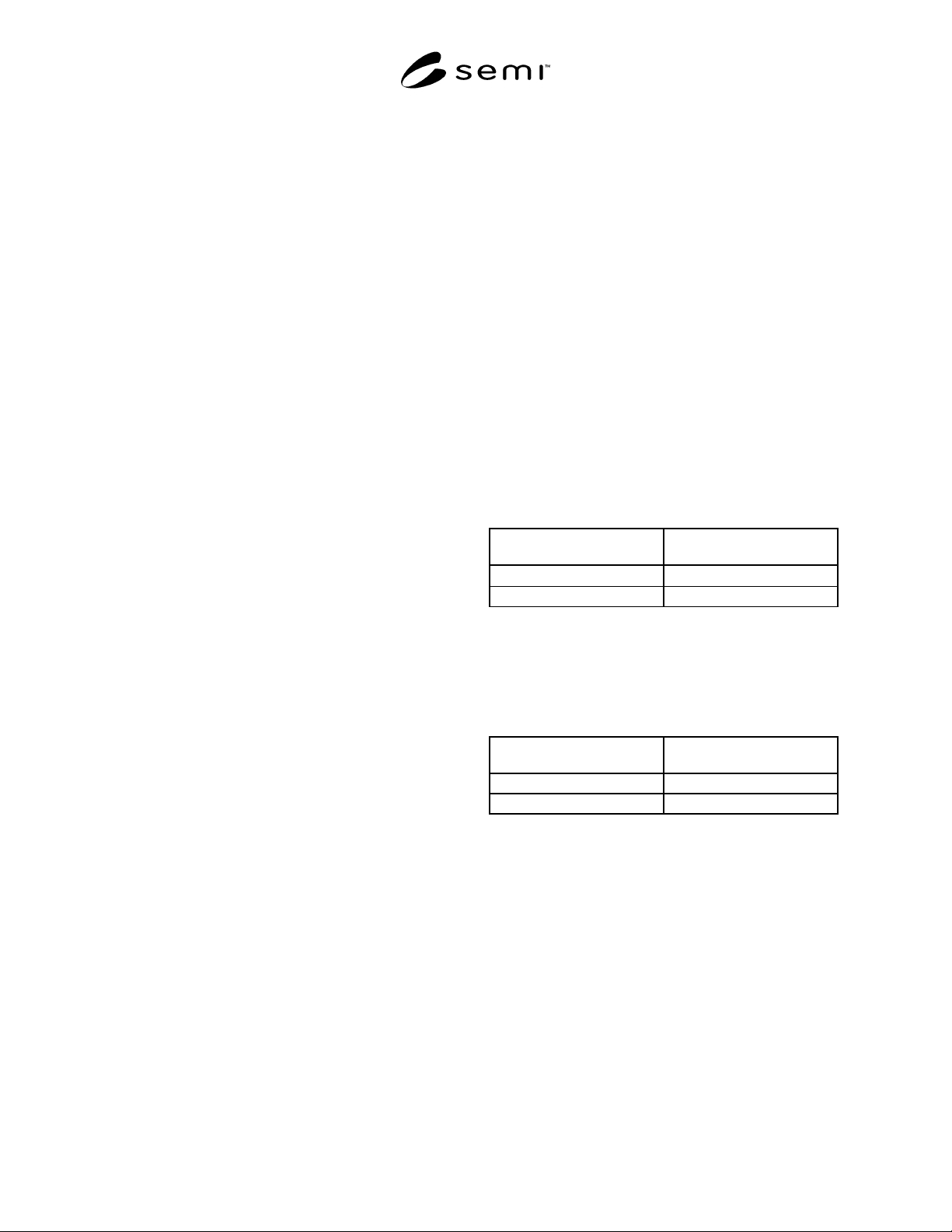
Table 4
Die Attach Area (Major
Dimension) inch (mm)
Flatness (Maximum
Allowable TIR) inch (mm)
0.750 (#=19.05)
0.002 (0.051)
>0.750 (>19.05) 0.003 inch ( 0.0762 mm)
7.1.5.3 Seal Area Flatness — See Table 5.
NOTE 10: These criteria apply to packages with bare ceramic,
metallized ceramic, or a metal ring. Flatness to be measured
per SEMI G6.
Table 5
Seal Ring (Major
Dimension) inch (mm)
Flatness (Maximum
Allowable TIR) inch (mm)
≤0.500 (≤12.7) 0.002 (0.051)
>0.500 (>12.7 ) 0.003 (0.076)
7.1.6 Delamination — Any evidenc e of delamination
between ceramic layers which exceeds 0.030" (0.762
mm), in a major dimension, in more than two locations.
NOTE 11: Inspection may also be made by scanning acoustic
microscopy per MIL-STD-883, Method 2030, if internal
delamination is suspected. Vendor and customer shall agree
that such inspection is necessary for package integrity.
7.1.7 Foreign Material — Any particulate or film-like
foreign material exceeding 0.005" (0.127 mm) height or
a surface dimension of 0.020" (0.508 mm). No more
than three acceptable sites allowed on the body with a
minimum separation of 0.030" (0.762 mm) required
between sites.