semi合集-English.pdf - 第6326页
3 SEMI G64-96 © SEMI 1996, 2004 7.7.2 Wire Bond — Agreed upon between user and supplier. 7.7.3 Solderab ility — The criteria for acceptable solderability are as follows: 1. The dipped portion of the samples is at le ast …
SEMI G64-96 © SEMI 1996, 2004 2
4.1.2 solderability — an index of the wettability and
coverage with solder of lead surface.
4.1.3 underplating — plating layers that complete the
required characteristics of the final plating layer and
lies between the base material and final plating layer.
5 Ordering Information
5.1 Priority
5.1.1 To avoid confusion, the order of precedence
when ordering leadframes shall be as follows:
1. Purchase Order (agreed between user and supplier)
2. This Specification
3. Referenced Documents
6 Materials
6.1 Base Material — Cu alloys or Fe/Ni alloys.
6.2 Plating Material — Underplating and Finish
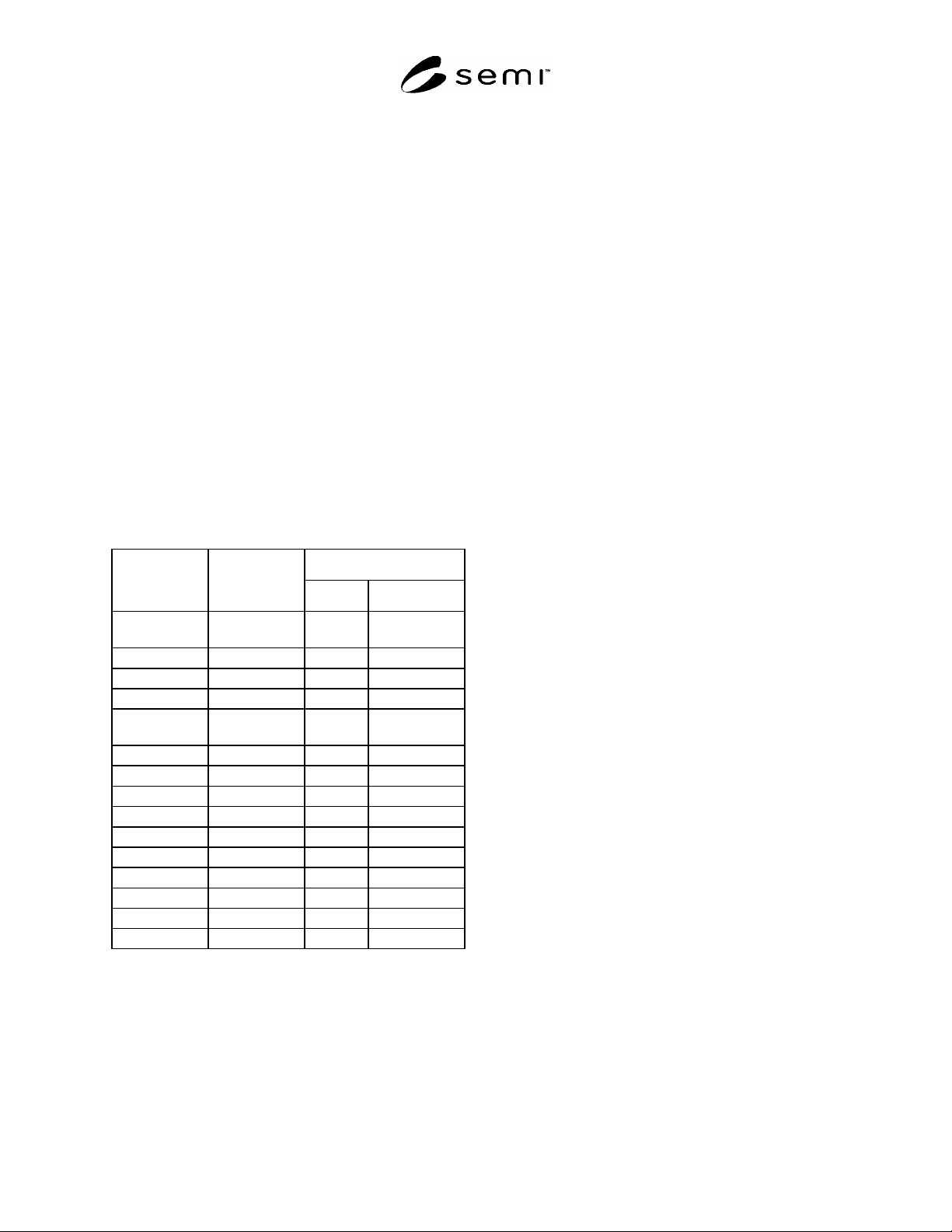
plating are shown in Table 1.
Table 1 Table 1 Underplating and Finish Plating
Base Material
Finish Plating Underplating
Cu-Alloys Fe, Ni-Alloys
Au (MIL-G-
45204)
- N/A X
Ni X X
Ag (QQS-365) - X N/A
Cu X X
Cu (MIL-C-
14550)
- X X
Ni X X
Ni (QQN-290) - X X
Cu X X
Pd/Ni-Alloy - X X
Ni X X
Cu X X
Pd - X X
Ni X X
Cu X X
Pd/Ni-Alloy X X
7 Plating Specification
7.1 Plating Thickness — For full-plated leadframes, the
designed thickness including under plating is restricted
as follows to limit the effects of thickness variation on
coplanarity and outer lead width.
Designed thickness including under plating-1 / Ag-
plating: 5 µm MAX
Designed thickness including under plating-2 / Au,
Cu, Ni, Pd/Ni-Alloy, Pd plating: 2 µm MAX
7.2 Visual Inspection — Rejectable conditions are as
follows:
1. Any bare spots, or missing plating in critical area as
defined the coined areas or minimum flat wire bond
area in the appropriate leadframe specification.
2. Any peeling or blistered plating.
3. Any nodules in critical area as defined the coined
areas or minimum flat wire bond area in the
appropriate leadframe specification.
NOTE 1: Nodules not exceeding 0.0381 mm in a surface
dimension and 0.0127 mm in height, in non-critical areas
are allowed providing there are no more than one per
internal lead finger or six (6) per leadframe.
4. Any pits which exceed 0.008 mm in depth or 0.0127
mm in a surface dimension in critical areas or
0.0254 mm in depth or 0.051 mm in a surface
dimension in non-critical areas.
5. Any scratches or scrapes in the metallization plating
which expose underplating or base material.
6. Any scratches or scrapes in critical area which cause
a build up of material in excess of 0.0127 mm in
height.
7. Any foreign material, contamination, or tarnish.
8. Non-uniformity or rough-plated surface.
7.3 Visual Inspection after Baking — The test
procedure is described in Section 9.3. Visual inspection
after baking shall be performed according to the
procedure in Section 9.2.1.
7.4 Corrosion Resistance (not applicable to Cu
plating) — In the test result, allowable corrosion
specification shall be agreed upon between user and
supplier.
7.5 Surface Ion Contamination — Allowable ion
species and ion concentration shall be agreed upon
between user and supplier.
7.6 Adhesion — If there is any plating film on the test
tape, the component shall be rejected. Adhesive test
should be performed according to the procedure in
Section 9.6.
7.7 Functional Tests
7.7.1 Die Attach — Agreed upon between user and
supplier.

3 SEMI G64-96 © SEMI 1996, 2004
7.7.2 Wire Bond — Agreed upon between user and
supplier.
7.7.3 Solderability — The criteria for acceptable
solderability are as follows:
1. The dipped portion of the samples is at least 95%
covered by a continuous solder coating.
2. Pinholes, voids, porosity, non-wetting, or dewetting
do not exceed 5% of total area.
NOTE 2: Solderability criteria for Ni and Cu plating are
established by the user and supplier and are excluded here.
8 Equipment
8.1 Fluorescent X-ray spectremeter
8.2 Binocular-microscope, 10–30× magnification
8.3 Neutral salt spray test equipment
8.4 Ion chromatography (Anion, Cation)
8.5 Hot plate or Heater block
8.6 Solder pot
8.7 Meniscograph
9 Sampling
9.1 Sampling plan shall be agreed upon between user
and supplier.
10 Test Methods
10.1 Thickness — Plating thickness shall be measured
by fluorescent X-ray spectrometer.
10.2 Visual Inspection
10.2.1 Magnification — Unless otherwise specified,
visually inspect the plating surface under a microscope
at 10× magnification. 30× magnification shall be used
for confirmation.
10.3 Baking Test
10.3.1 Baking Conditions — Samples are heated in air
on hot plates or heater block.
Table 2
Finish Plating/Base
Material
Cu-Alloys Fe/Ni-Alloys
Au* 450°C × 3 min. 450°C × 3 min.
Ag 300°C × 3 min. 400°C × 3 min.
Cu** 200°C × 1 hour 200°C × 1 hour
Ni** 400°C × 3 min. 400°C × 3 min.
Ni/Pd Alloy 200°C × 1 min. 200°C × 1 min.
Pd 300°C × 1 min. 300°C × 1 min.
* May be changed by agreement between user and supplier to 400°C
× 1 min or 450°C × 2 min or less, to account for changes in plating
thickness, base material, or other plating parameters.
** Surface oxidation and discoloration detected by visual inspection
are acceptable. Furthermore, parameter of solderbility evaluation for
flux, dipping method, etc. are to be determined by agreement between
user and supplier.
10.3.2 Visual inspection after baking shall be
performed according to the procedure in Section 9.2.1.
10.4 Corrosion Test — Atomize the test sample in a
test container using a 5% neutral sodium chloride
solution of 8.8–7.2pH at 35 ± 1°C for 24 hours. This
test follows ISO-9227.
10.5 Surface Ion Contamination — The measurement
follows SEMI G52.
10.6 Adhesion Test — Place the strip of tape
(SCOTCHª #540, #610, #810, or equivalent) across the
plated area. Press firmly with fingertips or other smooth
object. Peel the tape quickly off the plated surface. The
plating surface may be scored before the tape test in
accordance with the joint agreement between user and
supplier.
10.7 Functional Tests
10.7.1 Die Attach — Agreed upon between user and
supplier.
10.7.2 Wire Bond — Agreed upon between user and
supplier.
10.7.3 Solderability — The procedure for accelated
aging test shall be agreed upon between user and
supplier (see Appendix 1).

SEMI G64-96 © SEMI 1996, 2004 4
APPENDIX 1
SOLDERABILITY TEST
NOTICE: The material in this appendix is an official part of SEMI G64 and was approved by full letter ballot
procedures.
A1-1 Accelerated Environment Simulation
A1-1.1 Determination, due to the environment, may be
simulated by exposure to a hot plate that reproduces the
heat characteristics of assembly (a), and by steam aging
to simulate the storage environment. The following are
methods for accelerated environment simulations (b):
a. Place samples in air on a hot plate or a heat block.
Temperature and duration are detailed in Section
9.3, and represent the heat characteristics of
assembly.
b. Steam aging test is based on MIL-STD-883D,
Method 2003.7, and simulates environmental
conditions.
A1-2 Soldering Parameter
A1-1.2 Baked test specimens shall be dipped into flux
conforming to MIL-P-14256, type-R, for 5 to 10
seconds, and then dipped in a solder bath conforming to
QQ-S-571 for 10 ± 1 seconds at a solder pot
temperature of 230 ± 5°C.
A1-3 Evaluation of Solderability
A1-3.1 Wetting Area — After cleaning solder dipped
specimen with alcohol to remove flux, visually inspect
under a microscope at 10× magnification. Solder must
cover 95% or more of surface area, based on MIL-STD-
883D, Method 2003.7.
A1-3.2 Wetting Time (zero-cross-time) — Solder that
conforms to conditions below is evaluated according to
JIS-C-0053, or may be evaluated by a method
determined by user and supplier for certain leadframe
shapes.
1. Temperature: 230 ± 5°C
2. Dipping speed: 2 mm/second
3. Dipping depth: 2 mm
4. Flux: Rosin flux (MIL-F-14256, type-R)
5. Solder composition: 63 Sn / 37 Pb (QQ-S-571)
NOTICE: SEMI makes no warranties or
representations as to the suitability of the standards set
forth herein for any particular application. The
determination of the suitability of the standard is solely
the responsibility of the user. Users are cautioned to
refer to manufacturer's instructions, product labels,
product data sheets, and other relevant literature,
respecting any materials or equipment mentioned
herein. These standards are subject to change without
notice.
By publication of this standard, Semiconductor
Equipment and Materials International (SEMI) takes no
position respecting the validity of any patent rights or
copyrights asserted in connection with any items
mentioned in this standard. Users of this standard are
expressly advised that determination of any such patent
rights or copyrights, and the risk of infringement of
such rights are entirely their own responsibility.
Copyright by SEMI® (Semiconductor Equipment and Materials
International), 3081 Zanker Road, San Jose, CA 95134. Reproduction of
the contents in whole or in part is forbidden without express written
consent of SEMI.