semi合集-English.pdf - 第6375页
SEMI G72-0997 © SE MI 1997 2 6.2 The characteris tics classi ficati o n columns m ay be used in a data base format to sort the design l istings sequentially, top to bottom according to their sequential listing by column,…

SEMI G72-0997 © SEMI 19971
SEMI G72-0997
SPECIFICATION FOR BALL GRID ARRAY DESIGN LIBRARY
1 Purpose
The purpose of this specification is to promote industry
use of common BGA designs that may be distinguished
by their form, fit, function, and reliability requirements
and to record designs by category that meet these
requirements.
2 Scope
2.1 This document provides a library of company-
sponsored BGA designs for the purpose of promoting
the use of these common designs and to minimize the
unnecessary proliferation of new designs. New designs
will be added as they become sponsored by and
approved by member companies.
2.2 This library shall include ceramic, plastic, tape,
metal and other (as new categories of designs are
identified and added to this specification) BGA designs
that are fully compliant with existing JEDEC-registered
or standard mechanical outlines. Proposals for new
designs may be balloted in parallel with congruent
JEDEC registrations or standards, but will not be
published in this library until such registration and/or
standard is an approved JEDEC outline.
2.3 Controlling dimensions are metric (Systems
International units).
3 Referenced Documents
3.1 SEMI Documents
SEMI International Standards Compilation of Terms
Regulations Governing SEMI Standards Committees
3.2 ASME
1
ASME Y14.5M-94 — Dimensioning and Tolerancing
3.3 EIA/JEDEC
2
EIA JEDEC Publication 95 — Registered and Standard
Outlines for Semiconductor Devices
JEDEC BGA Design Guide 95-1 — Section 14
J-STD-020 —
1 American Society of Mechanical Engineers, 22 Law Drive,
P.O. Box 2900, Fairfield, New Jersey 07007-2900.
2 Electronic Industries Association, Joint Electron Device
Engineering Council, 2500 Wilson Blvd., Arlington, VA 22201,
(703) 907-7560.
JESD 22-A113 — Preconditioning of Plastic Surface
Mount Devices Prior to Reliability Testing
4 Terminology
4.1 ball grid array (BGA) package — A square or
rectangular substrate package with an array of metallic
balls on one surface of the package. The metallic balls
form the electrical and mechanical connection between
the package and the PC board or socket.
4.2 column grid array — Same as ball grid array
except that metallic columns are used in place of the
metallic balls for the electrical and mechanical
interconnection between the package and the PC board.
NOTE 1: In the text of this specification, whenever ball grids
are mentioned, a reference to column grids is also implied.
4.3 wire bond ring — Metalized area in the shape of a
complete or partial ring surrounding the die mounting
area intended for group electrical interconnections.
5 Ordering Information
5.1 Order of Precedence — To avoid conflicts, the
order of precedence when ordering ball grid array
substrates or assembled packages when using BGA
Library Designs from this specification shall be as
follows:
a. Purchase Order
b. Customer BGA Drawing
c. BGA Library Design from this specification
d. Referenced Documents from Section 3.0
e. Other related documents
6 General Design Character istics Listing
Format
6.1 Each design addition to this library shall include a
general design characteristics description which shall be
listed in Appendix 1 of this specification and also be
formatted on top of the title block for each design
drawing.
6.1.1 Description listings in the General Design
Characteristics, Appendix 1 shall be organized into
category sections: Plastic, Ceramic, Tape, Metal, or
Other.
6.1.2 These descriptions shall be listed across a row of
characteristics classification columns and may
determine the uniqueness of each design.

SEMI G72-0997 © SEMI 1997 2
6.2 The characteristics classification columns may be
used in a data base format to sort the design listings
sequentially, top to bottom according to their sequential
listing by column, left to right, in the following order.
These listings and their descriptive designations are as
follows:
6.2.1 Ball Count — List the actual number of balls on
the package.
6.2.2 Signal I/O — List the available balls for
individual signal I/O. This does not include balls that
are interconnected with other balls, bond rings, power
or ground planes or other electrically interconnected
features, such as die attach pads.
6.2.3 Body Size — List ##×## (i.e., 27×27) to
represent JEDEC Publication 95 registration values in
millimeters for “D” & “E” nominal body dimensions.
6.2.4 Pitch — List number representing JEDEC
Publication 95 registration values in millimeters for the
“e” pitch dimension.
6.2.5 Matrix — List ##×## (i.e., 20×20) to represent
JEDEC Publication 95 matrix values determined by the
number of balls on the outside row and column.
6.2.6 Array — List either Full, Staggered, Peripheral,
or Depopulated:
• Full — Completely filled matrix, as defined by the
JEDEC Publication 95 registration and variation
shown for each design.
• Staggered — A full matrix which has been
depopulated by every other ball in each row and
column.
• Peripheral — Balls missing in the center of the
BGA package. Outer rows of the matrix are fully
populated.
• Depopulated — Any variation not described by
full, staggered, or peripheral as described above.
NOTE 2: Any of the above matrix designs may have one ball
missing from its defined matrix description above, for
purposes of package orientation, and still be classified
according to that description.
6.2.7 Thermal Enhancement — List #×# (i.e., 6×6) or
“Cu Slug,” to designate either a specific matrix of balls
for thermal enhancement purposes or copper heat slug
for the same. Other metal slugs may be listed by their
appropriate metal constituent. List “N/A” if the design
has no thermal enhancement.
6.2.8 Profile Height — List the dimension of the
nominal profile height in millimeters.
6.2.9 Package Cavity Orientation — List either up or
down with reference to the board to which the package
design would be surfaced mounted (a cavity facing the
board would be cavity, down).
6.2.10 Wire bond Rings — List the number of wire-
bond rings. If the design has no rings, list “N/A.”
6.2.11 Substrate Materials — Generic description of
the materials the substrate is made from, excepting the
electrical trace and solder mask materials.
6.2.12 Metal Layers — The number of metal
interconnect layers in the BGA substrate. List a(bscpdg)
where:
a= total number of metal layers
b= number of signal layers
s= signal layer designator
c= number of power layers
p= power layer designator
d= number of ground layers
g= ground layer designator
e.g., 4(2slplg) would have 4 total layers made up of 2
signal layers and 1 power and ground layer each.
6.2.13 Die Interconnect — Interconnect method for
electrically connecting the die to the package. Normal
methods include wire bond, flip chip and TAB.
6.2.14 Encapsulation Design — Design description.
Normal categories are over-molded, liquid encapsulant
or lid.
6.2.15 Encapsulation Material — General description
of the material used to mechanically cover or
encapsulate the chip or die. The materials normally
used are epoxy for over-molding or liquid encapsulant
designs, metal, ceramic or laminate for lid designs.
6.2.16 Ball Composition — Description of the
material and composition of the ball. Should include a
percentage of tin/lead or other metals, if solder ball
(i.e., 63/37 Sn/Pb, alloy coated, copper or plastic).
6.2.17 JEDEC Designation — List JEDEC
designation from its Publication 95. This should include
registration or standard number, the specific variation
and revision designations (i.e., MO-151, BAE-1, B)
(this indicates Issue, Revision B).
6.2.18 Preconditioning Level — The specified
JEDEC, J-STD-020 moisture sensitivity performance
level requirement. This should also include a reference
to the revision of the J-STD-020 specification (e.g.,
Level 4, Revision A).
NOTE 3: JEDEC, JESD 22 - A113 specifies the moisture
preconditioning requirement for the moisture test to J-STD-
020.
SEMI G72-0997 © SEMI 19973
6.2.19 Design Number — SEMI assigned design
number for this design. The numbers will be assigned
by SEMI (upon ballot approval) and will be an
alphanumeric designation in sequential order as
follows:
• Plastic BGA Designs will be assigned PBDxxxx
designations, where xxxx numbers are sequentially
assigned beginning with 0001.
• Ceramic BGA Designs will be assigned CBDxxxx
designations, where xxxx numbers are sequentially
assigned beginning with 0001.
• Tape BGA Designs will be assigned TBDxxxx
designations, where xxxx numbers are sequentially
assigned beginning with 0001.
• Metal BGA Designs will be assigned MBDxxxx
designations, where xxxx numbers are sequentially
assigned beginning with 0001.
NOTE 4: The second letter designator may be assigned as
either a B or C to designate whether the design is a ball grid
or column grid array.
6.3 Appendix 1 is an example of a general design
characteristics listing for a plastic BGA.
7 Drawing Format
7.1 Appendix 2 is an example of the drawing format.
7.2 Dimensions
7.2.1 All dimensions, and tolerances shown or not
shown shall be in conformance with the JEDEC
Publication 95 registration or standard outline
referenced by the designation shown in the general
design characteristics listing for each design.
7.2.2 Nominal and basic dimensions shown in the
drawing may have minimum and maximum values and
associated tolerances that may be referenced in JEDEC
Publication 95 according to the registration designation
shown in the general design characteristics listing for
each design.
7.2.3 Dimension values will be shown on the drawing,
not in a table.
7.2.4 Basic dimensions only will be used for package
length and width dimensions (JEDEC “D” and “E”
dimensions), the ball pitch (JEDEC “e” dimension), and
the JEDEC “s” dimension.
7.2.5 The JEDEC “s” dimension will be shown only
for even row matrix designs. Odd row matrix designs
will only reference a centerline coincident with the
center of the center row of balls.
7.2.6 A nominal and maximum dimension for the
overall profile height (JEDEC dimension A) will be
shown. The maximum dimension shown may be less
than but may not exceed that maximum dimension
designated by the JEDEC Publication 95 registration
reference for this design.
7.2.7 Reference or nominal dimensions may be shown
for the package body thickness, substrate thickness,
encapsulation layer or lid thickness, and the standoff
height dimensions.
7.3 Ball Configurations
7.3.1 Retain and show the JEDEC method for
numbering the ball columns and rows.
7.3.2 The ball configuration drawing will show the
exact number and location of balls for each design.
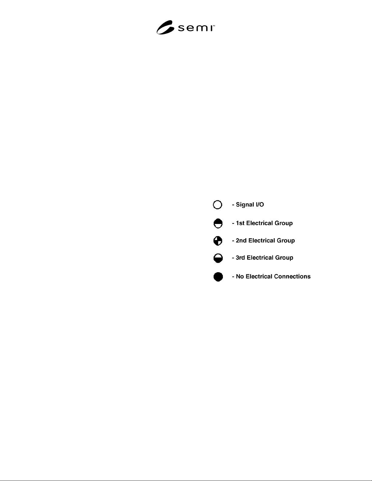
7.3.3 The following symbols are to be used for
designating the electrical interconnections or lack
thereof for the balls shown on the design drawing:
7.3.4 Notes on the drawing will show the above
symbols and designations for each of the electrical
groups used with each specific design.
7.4 The orientation of the internal bond finger
peripheral pad locations to the external package will be
illustrated by a top view of the package which indicates
the Pad 1 and A1 ball locations relative to the package
sides, 1–4, for all designs using wire bond or peri-
pheral die interconnection layout schemes.
7.4.1 For peripherally bonded layouts, the Pad 1 bond
finger will always be located in the same corner as the
A1 ball, and the pads will be sequentially numbered, for
purposes of the net list, in a counterclockwise rotation
as viewed from the die side of the substrate. This
applies to all cavity orientations (cavity up or down).
7.5 The design drawing must have a BGA design title,
a BGA design number, a revision number, the date of