semi合集-English.pdf - 第6377页
SEMI G72-0997 © SE MI 1997 4 issue an d a design page number shown at the bottom of each page. 7.6 The desi gn dra wing s hall i nclu d e a ge neral desi gn characteristics descriptio n which will also be listed in Appen…
SEMI G72-0997 © SEMI 19973
6.2.19 Design Number — SEMI assigned design
number for this design. The numbers will be assigned
by SEMI (upon ballot approval) and will be an
alphanumeric designation in sequential order as
follows:
• Plastic BGA Designs will be assigned PBDxxxx
designations, where xxxx numbers are sequentially
assigned beginning with 0001.
• Ceramic BGA Designs will be assigned CBDxxxx
designations, where xxxx numbers are sequentially
assigned beginning with 0001.
• Tape BGA Designs will be assigned TBDxxxx
designations, where xxxx numbers are sequentially
assigned beginning with 0001.
• Metal BGA Designs will be assigned MBDxxxx
designations, where xxxx numbers are sequentially
assigned beginning with 0001.
NOTE 4: The second letter designator may be assigned as
either a B or C to designate whether the design is a ball grid
or column grid array.
6.3 Appendix 1 is an example of a general design
characteristics listing for a plastic BGA.
7 Drawing Format
7.1 Appendix 2 is an example of the drawing format.
7.2 Dimensions
7.2.1 All dimensions, and tolerances shown or not
shown shall be in conformance with the JEDEC
Publication 95 registration or standard outline
referenced by the designation shown in the general
design characteristics listing for each design.
7.2.2 Nominal and basic dimensions shown in the
drawing may have minimum and maximum values and
associated tolerances that may be referenced in JEDEC
Publication 95 according to the registration designation
shown in the general design characteristics listing for
each design.
7.2.3 Dimension values will be shown on the drawing,
not in a table.
7.2.4 Basic dimensions only will be used for package
length and width dimensions (JEDEC “D” and “E”
dimensions), the ball pitch (JEDEC “e” dimension), and
the JEDEC “s” dimension.
7.2.5 The JEDEC “s” dimension will be shown only
for even row matrix designs. Odd row matrix designs
will only reference a centerline coincident with the
center of the center row of balls.
7.2.6 A nominal and maximum dimension for the
overall profile height (JEDEC dimension A) will be
shown. The maximum dimension shown may be less
than but may not exceed that maximum dimension
designated by the JEDEC Publication 95 registration
reference for this design.
7.2.7 Reference or nominal dimensions may be shown
for the package body thickness, substrate thickness,
encapsulation layer or lid thickness, and the standoff
height dimensions.
7.3 Ball Configurations
7.3.1 Retain and show the JEDEC method for
numbering the ball columns and rows.
7.3.2 The ball configuration drawing will show the
exact number and location of balls for each design.
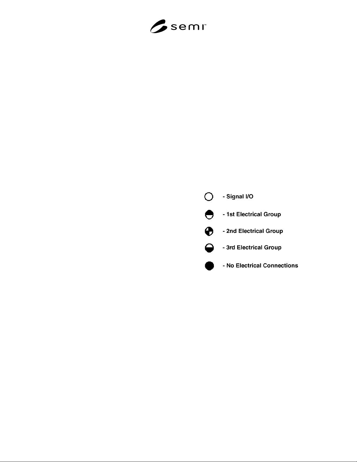
7.3.3 The following symbols are to be used for
designating the electrical interconnections or lack
thereof for the balls shown on the design drawing:
7.3.4 Notes on the drawing will show the above
symbols and designations for each of the electrical
groups used with each specific design.
7.4 The orientation of the internal bond finger
peripheral pad locations to the external package will be
illustrated by a top view of the package which indicates
the Pad 1 and A1 ball locations relative to the package
sides, 1–4, for all designs using wire bond or peri-
pheral die interconnection layout schemes.
7.4.1 For peripherally bonded layouts, the Pad 1 bond
finger will always be located in the same corner as the
A1 ball, and the pads will be sequentially numbered, for
purposes of the net list, in a counterclockwise rotation
as viewed from the die side of the substrate. This
applies to all cavity orientations (cavity up or down).
7.5 The design drawing must have a BGA design title,
a BGA design number, a revision number, the date of

SEMI G72-0997 © SEMI 1997 4
issue and a design page number shown at the bottom of
each page.
7.6 The design drawing shall include a general design
characteristics description which will also be listed in
Appendix 1 of this specification. This description
should be re-formatted on top of the title block for each
design drawing and may exclude the BGA design
number, which will be shown in the title block at the
bottom of the page.
8 Net List Format
8.1 Appendix 3 is an example of the net list format
including all reference notes.
8.2 The net list shall follow the drawing as part of the
BGA design and shall be formatted in columns as
follows:
• Column 1: Lists BGA wire bond pad and wire bond
ring numbers.
• Column 2: Lists solder ball connections.
• Column 3: Open column for later use in listing die
wire bond pad numbers.
• Column 4: Open column for later use in listing die
I/O name.
• Column 5: Lists package side location number of
bond pad connection.
• Column 6: Lists note reference numbers.
8.2.1 The listing of ball numbers should begin with
A1, and continue in sequential order (i.e., A1, A2...An,
B1, B2...Bn, C1, C2...Cn).
8.2.2 Wire bond ring numbers in the first column
should be designated in sequential order from inner
most to outermost (i.e., w/b ring 1, w/b ring 2, and w/b
ring 3) if there are three separate rings. The innermost
ring being w/b ring 1 and the outermost ring being w/b
ring 3.
8.3 Notes in the net list will reference each of the
electrical groups used with that specific design and will
list all additional associated interconnections for those
groups, if any.
8.4 Notes may consist of explanation of bond finger
orientation relative to top view illustration on drawing
for reference (independent of general specification
explanations) of net list to BGA design drawing.
8.5 Notes may also consist of applications warnings or
guidelines to insure correct use of the net list with the
design drawing.
8.6 All pages of net list must have a BGA design title,
a BGA design number, a revision number, the date of
issue and a design page number shown at the top of
each page.
9 Addition of Registrations
9.1 This specification will be published initially in a
loose leaf notebook and as package design registrations
are approved, they will be individually published in a
loose leaf format for easy access into the original
notebook by the publication owner.
9.2 Each new registration must be added to the
specification using the SEMI standard balloting
procedures. Refer to the “Regulations Governing SEMI
Standards Committees” publication.
NOTICE: These standards do not purport to address
safety issues, if any, associated with their use. It is the
responsibility of the user of these standards to establish
appropriate safety and health practices and determine
the applicability of regulatory limitations prior to use.
SEMI makes no warranties or representations as to the
suitability of the standards set forth herein for any
particular application. The determination of the
suitability of the standard is solely the responsibility of
the user. Users are cautioned to refer to manufacturer’s
instructions, product labels, product data sheets, and
other relevant literature respecting any materials
mentioned herein. These standards are subject to
change without notice.
The user’s attention is called to the possibility that
compliance with this standard may require use of
copyrighted material or of an invention covered by
patent rights. By publication of this standard, SEMI
takes no position respecting the validity of any patent
rights or copyrights asserted in connection with any
item mentioned in this standard. Users of this standard
are expressly advised that determination of any such
patent rights or copyrights, and the risk of infringement
of such rights, are entirely their own responsibility.
Copyright by SEMI® (Semiconductor Equipment and Materials
International), 3081 Zanker Road, San Jose, CA 95134. Reproduction o
f
the contents in whole or in part is forbidden without express written
consent of SEMI.
SEMI G72.1-0997 © SEMI 19971
SEMI G72.1-0997
DESIGN PROPOSAL FOR BALL GRID ARRAY DESIGN LIBRARY:292
PIN PLASTIC BALL GRID ARRAY
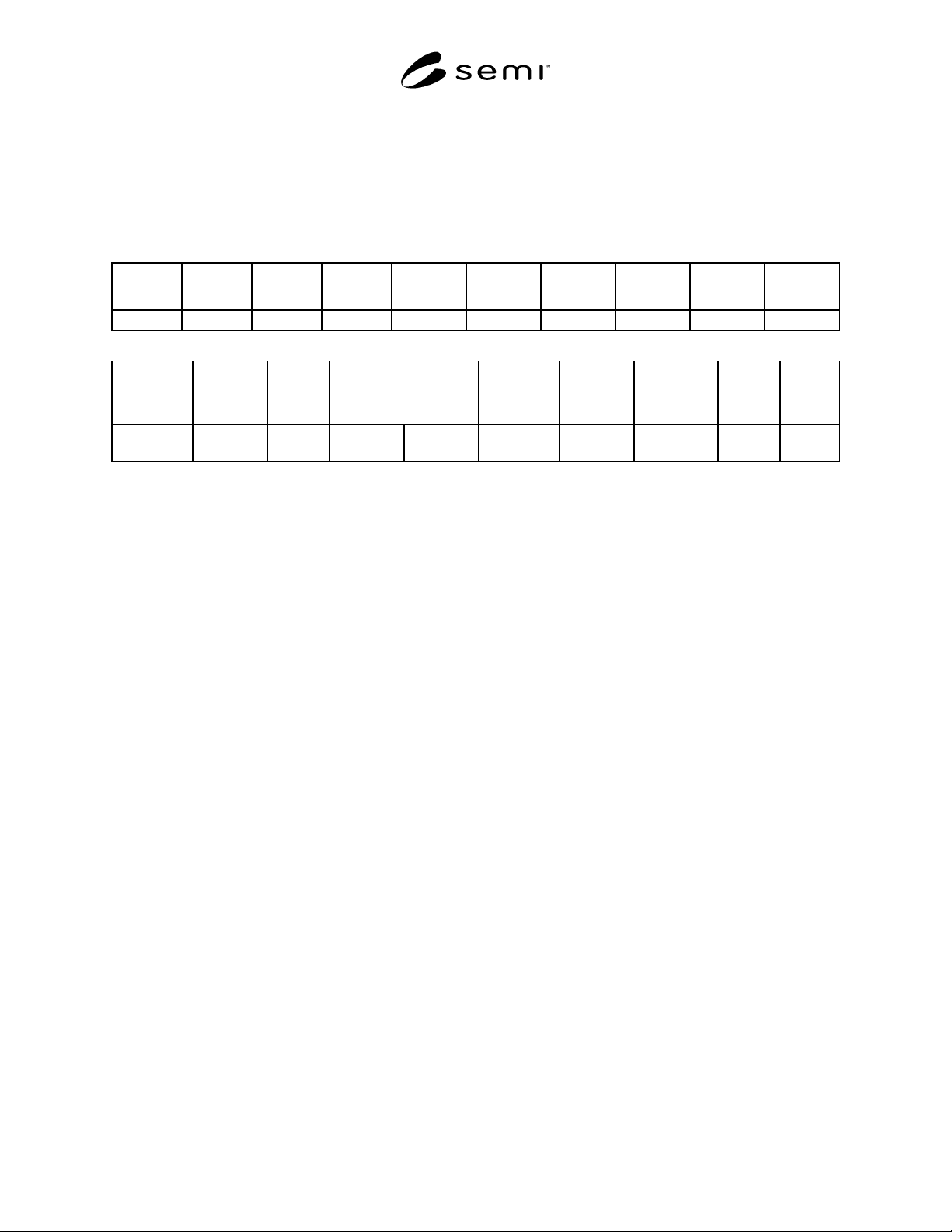
Table 1 Plastic Ball Grid Array (PBGA) General Design Characteristics
Ball Count Signal I/O Body Size Pitch Matrix Array
Thermal
Enhan.
Profile
Height
Cavity
Orient.
Wirebond
Rings
292 231 27x27 1.27 20x20 depopulated 6x6 2.13 up 2
Substrate
Material
Metal
Layers
Die Inter-
connect
Encapsulation
Design / Material
Ball
Composition
JEDEC
Designation
Precondition-
ing Level
Design
No.
SEMI
Designa-
tion No.
BT Laminate 2(2S0P0G) wirebond overmolded epoxy 63/37 Sn/Pb MO-151
BAL-2, B
Level 3,Rev 0 PBD0001 G72.1