semi合集-English.pdf - 第6490页
SEMI G79-0200 © SE MI 2000 3 6.2.4 Examination of the OTA defin i t io n in the con- text of F igure 1, that being the general case and not a single poin t timing evaluation, reveals that the overall timing accuracy time…
SEMI G79-0200 © SEMI 2000 2
NOTE 1: The term “input” as it appears in this document
refers to the device under test.
6 Test Methods
6.1 See Figure 1.
NOTE 2: A verification procedure to complement this Overall
Digital Timing Accuracy Specification is currently being
developed as a SEMI draft document.
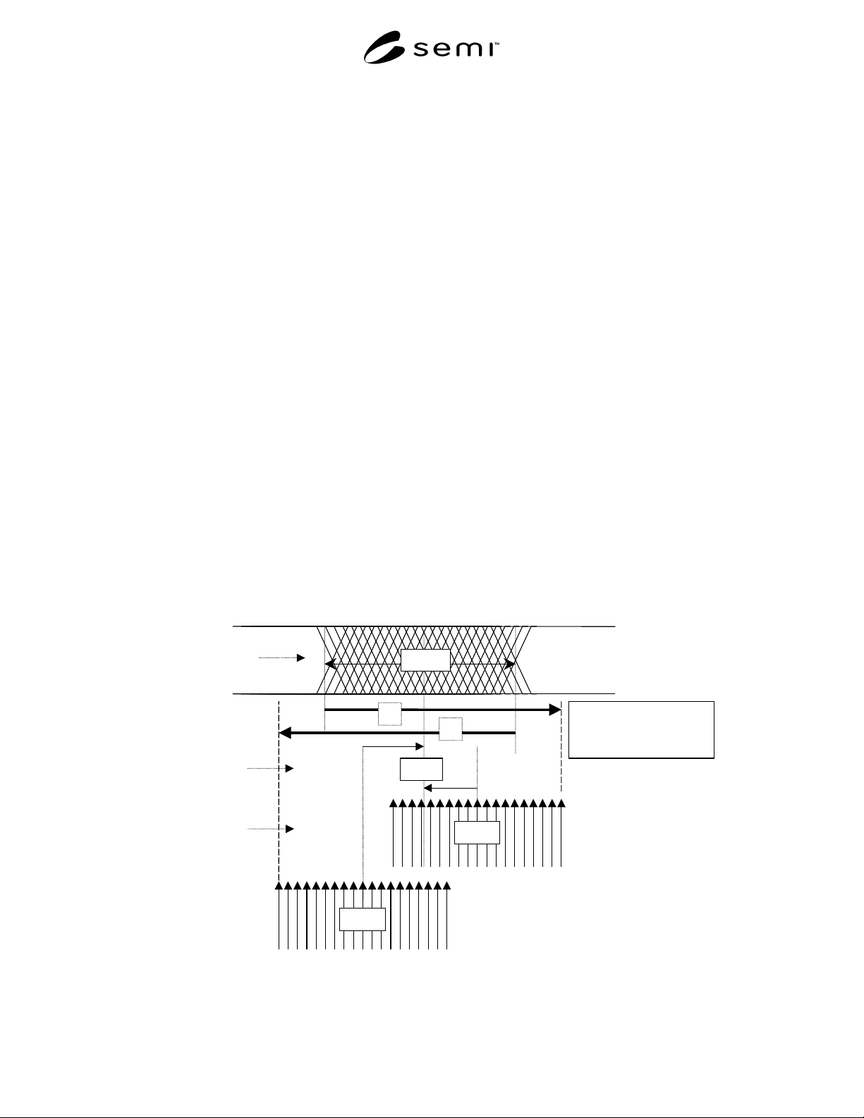
6.2 Explanation of Figure 1 — This figure is meant to
graphically describe Overall Timing Accuracy and its
constituent components. Overall Timing Accuracy
(OTA) is made up of three components, and by
definition is the aggregate timing error comprised of
input edge placement accuracy (see Section 7.1.1),
output edge placement accuracy (see Section 7.1.2), and
input to output timing accuracy (see Section 7.1.3). It’s
important to note that the OTA specification and
associated graphical representation shown in Figure 1 is
meant to encompass timing delay errors across multiple
machines, as well as multiple calibrations for a single
machine over time.
6.2.1 Our experience in dealing with multiple-pin
automated test systems reveals that not all input drive
circuits can place a drive edge at exactly the same point
in time relative to a common reference. The same is
true for output compare circuits when placing compare
edges. Thus, these edges tend to have an (error)
distribution around some average value relative to their
intended placement. This is due in part to the inherent
anomalies associated with electronic circuits that make-
up these edge placement elements. The distribution of
edge error is graphically shown for input (see Section
7.1.1) and output edge (see Section 7.1.2) signals in
Figure 1.
6.2.2 Drive Input to Compare Output Timing
Accuracy (Section 7.1.3) can be described in different
ways. It is easy to think of this parameter, per the
definition given in this document, Section 7.1.3, as
simply the relative time difference (skew) between the
drive delay timing error distribution and the compare
delay timing error distribution for a particular machine.
But this parameter, once established for a machine, is
not necessarily constant. For example, this parameter
can change from one calibration of a machine at a
particular time, to something different, as a result of a
subsequent calibration of that same machine. As well,
this parameter can also be considered as a machine to
machine accuracy parameter, not necessarily having the
same value between any two machines of the same
kind.
6.2.3 Thus, on each machine and at different points in
time for the same machine the Drive Input to Compare
Output Timing skew can be uniquely different per
machine. That difference being influenced by the
various machine anomalies that contribute to machine
error including the not so perfect results of a periodic
edge calibration.
7.1.2
Input to Output Timing
Accuracy (7.1.3)
Output Edge Placement
Accuracy (7.1.2)
7.1.3
Input Edge Placement
Accuracy (7.1.1)
7.1.1
Output delay timing error- For another machine,
or a new spread for the same machine as a result
of a calibration.
7.1.2
Output timing delay
error.
A
B
Overall Timing Accuracy
(+A, -B)
Figure 1
Overall Timing Accuracy

SEMI G79-0200 © SEMI 20003
6.2.4 Examination of the OTA definition in the con-
text of Figure 1, that being the general case and not a
single point timing evaluation, reveals that the overall
timing accuracy time value is the time line indicated by
“A” and the time line indicated by “B”. In a single
point AC timing evaluation, OTA is determined as a
distribution of edges associated with time line “A” or
time line “B”, depending upon the relationship between
the drive edge values and compare edge values (see
Section 7.1.3) at that point in time.
7 Definitions
7.1 Overall Timing Accuracy — aggregate timing
error comprised of input edge placement accuracy,
output edge placement accuracy and input to output
timing accuracy. (See Figure 1.)
7.1.1 Input Edge Placement Accuracy — DUT input
timing error comprised of input timing delay error,
input timing jitter and input transition time variation.
7.1.1.1 Input Timing Delay Error @ 5V — time delay
error at the midpoint of a 5V transition, with respect to
an ideal delay (NIST traceable delay reference), using
any pin, any delay value, any input timing edge, any
format (NR, Rtx, SBx), positive or negative transition
and any test cycle length.
Conditions:
• delays are normalized to pin 1 (first tester pin),
rising edge, NR format, @ 0ns;
• errors are normalized to the average of minimum
and maximum of the error distribution;
1
• reference load A; and
• physical reference point is a zero length
interconnect on the DUT side of a standard
performance board.
7.1.1.2 Input Timing Delay Error @ 3V — (same as
Section 7.1.1.1 @ 3V)
7.1.1.3 Input Timing Delay Error @ 1V — (same as
Section 7.1.1.1 @ 1V)
7.1.1.4 Input Timing Jitter — short term (cycle to
cycle) instability using any pin, any input timing edge,
any format (NR, RTx, SBx).
Conditions:
• error expressed as RMS value;
• reference load B;
1 “Average of min and max of the error distribution” is defined as:
(min error + max error)/2. This can also be referred to as “center
of spread”.
• physical reference point is a zero length intercon-
nect on the DUT side of a standard performance
board; and
• error referenced to corresponding transition of
prior cycle.
7.1.1.5 Input Transition Time Variation @ 5V —
minimum and maximum rise and fall times of a 5V
input signal transition using any pin.
Conditions:
• referenced to the time variation between the 20%
and 80% points of both positive and negative
signal transitions;
• reference load A; and
• physical reference point is a zero length intercon-
nect on the DUT side of a standard performance
board.
7.1.1.6 Input Transition Time Variation @ 3V —
(same as Section 7.1.1.5 @ 3V)
7.1.1.7 Input Transition Time Variation @ 1V —
(same as Section 7.1.1.5 @ 1V)
7.1.2 Output Edge Placement Accuracy — DUT
output compare timing error comprised of output timing
delay error and output compare timing jitter.
7.1.2.1 Output Timing Delay Error @ 5V — time
delay error at the detected midpoint of a 5V transition,
with respect to an ideal delay (NIST traceable refer-
ence), using any pin, any delay value, any compare
timing edge, window or strobe compare mode, expect H
or L, positive or negative transition and any test cycle
length.
Conditions:
• measured with load circuit “off” or high
impedance;
• delays normalized to rising edge detected by pin 1
(first tester pin), using strobe compare format,
expect H @ 0ns;
• error normalized to the average of minimum and
maximum of the error distribution; and
• input signal: 50-ohm source, 0–5V step, > 1V/ns,
inserted at a zero length interconnect on the DUT
side of a standard performance board.
7.1.2.2 Output Timing Delay Error @ 3V— (same as
Section 7.1.2.1 using 3V input signal)
7.1.2.3 Output Timing Delay Error @ 1V — (same as
Section 7.1.2.1 using 1V input signal)

SEMI G79-0200 © SEMI 2000 4
7.1.2.4 Output Timing Jitter— short term (cycle to
cycle) instability using any pin, any compare timing
edge, window or strobe compare mode, expect H or L.
Conditions:
• error expressed as RMS value;
• physical reference point is a zero length intercon-
nect on the DUT side of a standard performance
board; and
• jitter referenced to an independent synchronous
trigger.
7.1.3 Input to Output Timing Accuracy — relative
time difference between the average of minimum and
maximum drive input delay timing and the average of
minimum and maximum compare output delay timing.
7.1.3.1 Input to Output Timing Error @ 5V — relative
time difference between the average of minimum and
maximum input delay timing error @ 5V (Section
7.1.1.1) and the average of minimum and maximum
output timing delay error @ 5V (Section 7.1.2.1).
Conditions:
• (same as Sections 7.1.1.1 and 7.1.2.1).
7.1.3.2 Input to Output Timing Error @ 3V — same as
Section 7.1.3.1 using 3V input signal and definitions/
conditions specified in Sections 7.1.1.2 and 7.1.2.2.
7.1.3.3 Input to Output Timing Error @ 1V — same as
Section 7.1.3.1 using 1V input signal and definitions/
conditions specified in Sections 7.1.1.3 and 7.1.2.3.
7.1.4 High Speed Clock Accuracy — DUT high speed
clock input timing error (if different than normal tester
input channels) comprised of high speed clock delay
error, high speed clock self-trigger cycle jitter, high
speed clock self-trigger phase jitter and high speed
clock transition time variation.
7.1.4.1 High Speed Clock Delay Error @ 5V — time
delay at the midpoint of a 5V transition, with respect to
an ideal delay (NIST traceable delay reference), using
any pin, any delay value, any input timing edge, RTZ
format, and any test cycle length.
Conditions:
• delays are normalized to pin 1 (first tester pin),
rising edge, NR format, @ 0ns;
• errors are normalized to the average of minimum
and maximum of the error distribution;
• reference load A; and
• physical reference point is a zero length intercon-
nect on the DUT side of a standard performance
board.
7.1.4.2 High Speed Clock Delay Error @ 3V — (same
as Section 7.1.4.1 @ 3V)
7.1.4.3 High Speed Clock Delay Error @ 1V — (same
as 7.1.4.1 @ 1V)
7.1.4.4 High Speed Clock Self-trigger Cycle Jitter —
short term instability using any high speed clock pin,
from a rising clock edge to the next rising clock edge,
or falling clock edge to the next falling clock edge.
Conditions:
• error expressed as RMS value;
• reference load B; and
• physical reference point is a zero length
interconnect on the DUT side of a standard
performance board.
7.1.4.5 High Speed Clock Self-trigger Phase Jitter —
short term instability using any high speed clock pin,
from a rising clock edge to the next falling clock edge,
or falling clock edge to the next rising clock edge.
Conditions:
• error expressed as RMS value;
• reference load B; and
• physical reference point is a zero length
interconnect on the DUT side of a standard
performance board.
7.1.4.6 High Speed Clock Transition Time Variation
@ 5V — minimum and maximum rise and fall times of
a 5V input signal transition using any high speed clock
pin.
Conditions:
• referenced to the 20% and 80% points of a positive
and negative signal transition;
• reference load A; and
• physical reference point is a zero length
interconnect on the DUT side of a standard.
7.1.4.7 High Speed Clock Transition Time Variation
@ 3V — (same as Section 7.1.4.6 @ 3V)
7.1.4.8 High Speed Clock Transition Time Variation
@ 1V — (same as Section 7.1.4.6 @ 1V)
7.1.5 Input Timing Delay Error for Z to Drive
High/Low — Time delay error at the midpoint of a
driver transition from Z to high/low, with respect to an
ideal delay, using any pin, any delay value, any Z