semi合集-English.pdf - 第6497页
SEMI G80-0200 © SE MI 2000 5 equipment interaction accomm odated by the application program i s necessary for data collection at Level 2. 10.3 Level 1 Tes ts — Le vel 1 tests a r e i ntended to efficiently g at her a lar…
SEMI G80-0200 © SEMI 2000 4
performed and the equipment is to be configured for
normal and intended operation.
9.3 Supplemental Equipment Calibration — External
equipment used for level 2 data collection in this
procedure must be verified for proper calibration.
10 Test Method Procedure
10.1 The procedure is comprised of Level 1 tests and
Level 2 tests. Any ATE capability described in the
following tests that is not available on the ATE under
analysis is not required for compliance to the
procedure, but should be noted in the verification
results Table 1 and Table 2.
10.2 Each test system is different; thus this procedure
is generic. Regardless, it will provide comprehensive
results when the specific application is created using
this procedure as a guide. Per the requirements, a load
board and application program written to accommodate
the procedure should be in place when the procedure is
executed. This procedure is to be executed per the
requirements outlined in Section 7 of this document.
When these requirements are met, the following steps
will comprise the step by step process for execution of
this Test Method:
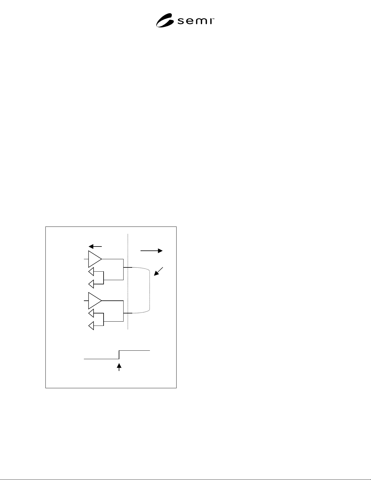
Adjacent pins shorted together
Pin n
Pin n+1
Short
Pin n
Driver
Receiver
Pin n+1
Driver
Receiver
Tester
Performance
b
oard
Pairs of adjacent tester pins are shorted together with
a
minimum length interconnect on the performance board.
Figure 1
Level 1 Verification
1. Install the performance board.
2. Power up the system and supplemental equipment,
allow adequate time for stabilization.
3. Load the appropriate application program that
represents the embodiment of the procedure called out
in Sections 10.3.1, 10.3.4, 10.3.5, and 10.3.6 for Level
1 as well as Sections 10.4.1, 10.4.2, 10.4.3, 10.4.4,
10.4.5, and 10.4.6 for Level 2.
4. Execute the method to completion. The application
program can capture the data for Level 1 and Level 2
and store that for later analysis.
5. This procedure calls for various time measurements
to be made at specified voltage points or signal levels.
The user is encouraged to maintain these values to keep
the method results constants when system to system
comparisons are being made. Regardless, he is free to
adjust these measurement points or levels to accommo-
date specific integrated circuit technology requirements
important to that product and the system being
analyzed. When that occurs documentation of those
procedure variations must be entered in Appendix 3
(Exceptions Page).
6. Best results from this procedure are achieved if a
consistent measurement methodology is maintained.
This is important when making time measurements
relative to a particular transition point on a signal edge.
This method recommends that when signal measure-
ments are specified at a particular transition point, i.e.,
50%, that this point on the edge be determined relative
to the 0% or 100% steady state levels displayed on the
oscilloscope, after any aberrations due to the transition
have expired. A tester reference channel, the lowest
channel, should be used to set the measurement point(s)
and then consistently used as the basis for subsequent
measurements for the remaining tester channels.
7. Data Analysis –– Analyze the captured data and
make the appropriate data entries to Table 1, provided
in this method document.
8. When this method execution is complete, document
all method exceptions in the EXCEPTIONS section of
this document (Appendix 3).
9. Results –– Data entry to Table 2. Make the
appropriate data entries to Table 2, provided in this
method document and supplemented with examples
contained in Appendix 2.
10.2.1 Level 1 requires no external equipment for
completion, whereas Level 2 does require use of
external equipment. The user is free to implement this
procedure through total manual intervention. On the
other hand, the user may choose to apply an automated
or robotic approach to data collection for Level 2.
Regardless, the user is advised that tester and external
SEMI G80-0200 © SEMI 20005
equipment interaction accommodated by the application
program is necessary for data collection at Level 2.
10.3 Level 1 Tests — Level 1 tests are intended to
efficiently gather a large amount of data by taking
advantage of the self-analysis ability of the ATE. This
is accomplished by shorting adjacent tester channels
together on a performance board with minimum, equal
length interconnections, and using one channel to test
the other. Reference Figure 1. Execution speed and
system resource coverage are of primary importance for
Level 1. Level 1 is intended to analyze specification
conformance as opposed to diagnose system failures.
All measurements are normalized to “zero” in order to
facilitate subsequent data reduction/analysis. Level 1 is
intended to collect data only. Data reduction and
processing are to be done off-line in order to maximize
data collection efficiency.
10.3.1 Timing Linearity Test — This test is used to
establish drive input to compare output timing accuracy
by “stretching” the test cycle in minimum cycle
programming increments while using fixed percentage
delays and pulse widths as the method sweeps through
various timing conditions. The test pattern should be
written to switch all even or odd pins simultaneously,
and for all transitions and associated strobes to occur at
least 100 times for each data point.
10.3.2 For clarification all drive edges are detected in
parallel in pairs. The intention is to sweep the compare
edge and detect the earliest occurrence of a drive edge
with the latest compare edge, as well as detect the latest
occurrence of a drive edge with the earliest compare
edge.
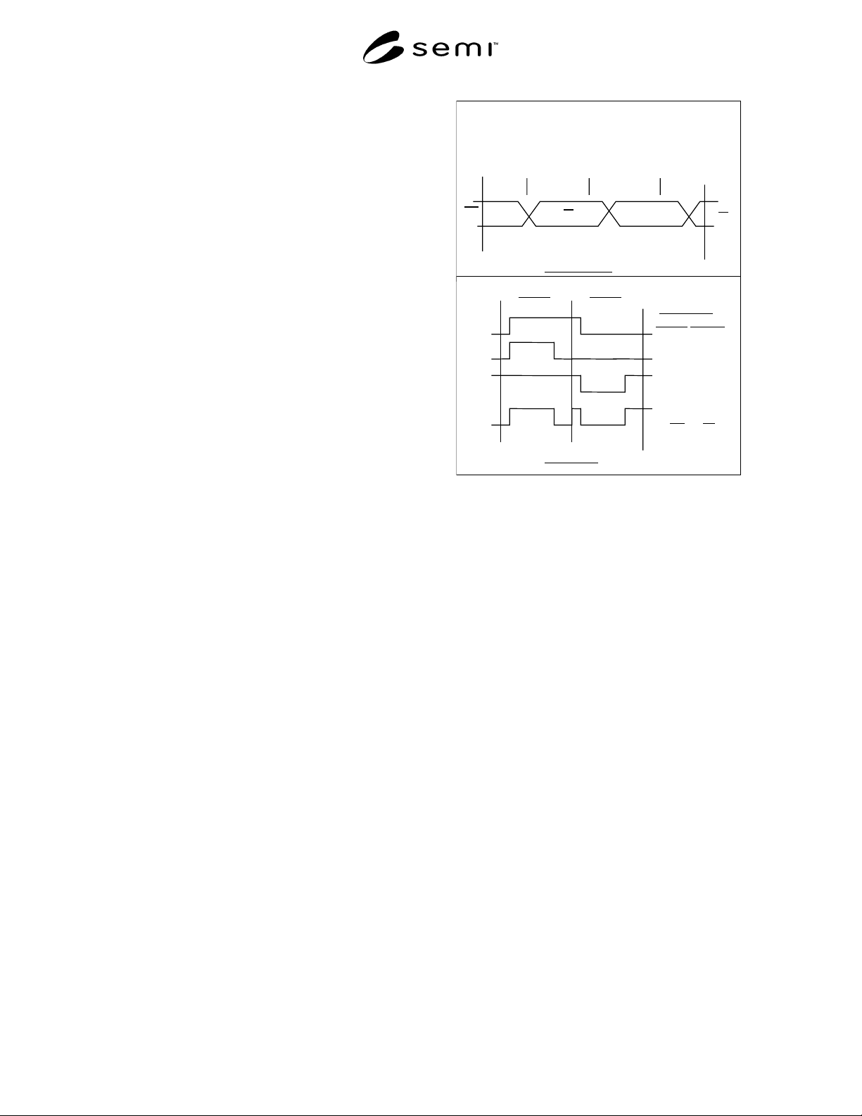
SBC Example
For pulse width = 33.3% (SBC
format) all formats start at 25% of the
programmed test cycle.
25% 33% 33%
25% 50% 75% 100% 0
DD
D
D
Data 1 Data 0
N
R
RTZ
RTO
SBC
Transitions
Data 1 Data 0
1 1
2 0
0 2
3
3
total: 6 6
Transitions
Figure 2
SBC Example and Transitions
10.3.3 The following Test Cycle Example and nested
loop outline describes the test flow:
for amplitude = 1V, 3V, 5V
for direction =
odd_pins_drive_&_even_pins_compare to
even_pins_drive_&_odd_pins_compare
for test_cycle = min_cycle to [min_cycle +
500*cycle_resolution] by
cycle_resolution, 3x min_cycle, 10x min cycle
for pulse width = 50% (RTZ/RTO formats)
= 33.3% (SBC format)
= don't care (NR format)
for format = NR, RTZ, RTO, SBC (NOTE 1: all
formats start at 25% of the programmed test
cycle)
for all format transitions (pattern data 0 and 1)
detect earliest occurrence of format
transition midpoint with the latest
compare pin
detect latest occurrence of format transition
midpoint with the earliest compare pin
error = (latest occurrence - earliest
occurrence)
end transitions
end format
end pulse width
end test_cycle
end direction
end amplitude
SEMI G80-0200 © SEMI 2000 6
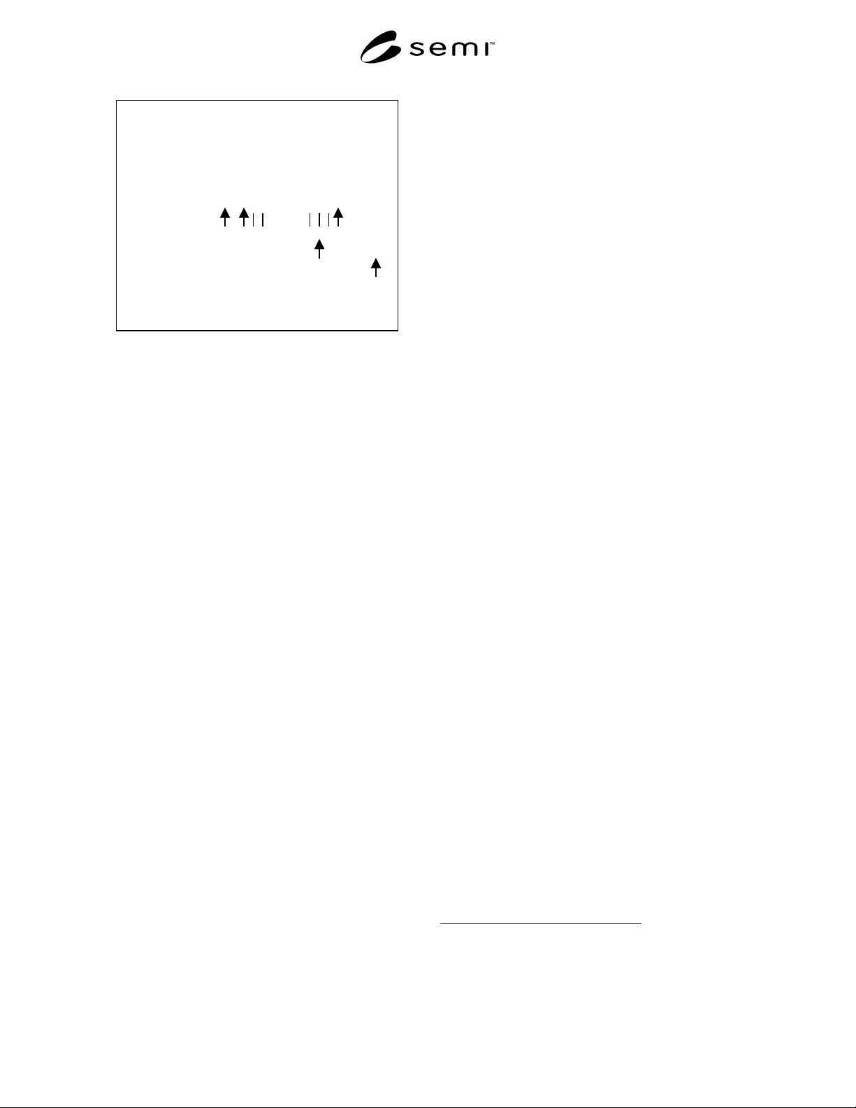
0 10ns 35ns
• 1 cycle: 3X = 30ns
•
1 cycle: 10X = 100ns
Total of 503 cycles. The intention of the last two cycles is
to define a period that is far beyond the minimum period.
Period resolution: 50ps
Minimum Period Cycle: 10ns
10ns to (10ns + 25ns) by 50ps
•
501 cycles:
For test_cycle = min_cycle to [min_cycle + 500*cycle
resolution] by cycle_resolution, 3Xmin_cycle, 10x min_cycle.
30ns
100ns
Example:
Figure 3
Test Cycle Example
10.3.4 Extended Delay Test — This test is used to
establish drive input to compare output timing accuracy
when timing generator delay values are programmed
beyond the length of the test cycle. Driver input delays
are programmed to occur in subsequent test cycles and
detected with compare delays originating in the corres-
ponding subsequent test cycle. The intention is the
same as Section 10.3.1 with the exception that edges
are programmed into a subsequent cycle. Conditions
such as formats and voltages have been reduced to keep
the amount of data collected down to a reasonable level.
10.3.4.1 The following nested loop outline describes
the test flow:
for amplitude = 3V
for direction =
odd_pins_drive_&_even_pins_compare to
even_pins_drive_&_odd_pins_compare
for test_cycle = min to 10*min by 0.1*min
for format = NR
for format_delay = test_cycle to max_delay by
0.25*test_cycle (max delay is beyond the cycle
boundary)
detect earliest occurrence of format
transition midpoint with the latest
compare pin using pattern expect
data shifted into the appropriate cycle
detect latest occurrence of format transition
midpoint with the earliest compare pin
using pattern expect data shifted into
the appropriate cycle
error = (latest occurrence - earliest
occurrence)
end delays
end format
end test cycles
end directions
end amplitude
10.3.5 Driver Z State Test — This test verifies the
timing accuracy of tester driver transitions from Z to
1/0 and from 1/0 to Z. Driver inputs are programmed to
transition to and from Z and 1/0 while being loaded
with 50 ohms terminated to drive 1 for Z to 0 and 0 to
Z, and 50 ohms terminated to drive 0 for Z to 1 and 1 to
Z
7
(reference load C). The following nested loop
outline describes the test flow:
for amplitude = 3V
for direction =
odd_pins_drive_&_even_pins_compare to
even_pins_drive_&_odd_pins_compare
for test_cycle = 5*min_cycle
for format_delay = 50%
for format = NR
detect earliest occurrence of Z to low tran-
sition at scaled midpoint with compare pins
detect latest occurrence of Z to low tran-
sition at scaled midpoint with compare pins
error=(latest occurrence - earliest occurrence)
detect earliest occurrence of Z to 1 tran-
sition at scaled midpoint with compare pins
detect latest occurrence of Z to 1 transition
at scaled midpoint with compare pins
error = (latest occurrence - earliest occur-
rence)
detect earliest occurrence of 0 to Z transition
at scaled midpoint with compare pins
detect latest occurrence of 0 to Z transition at
scaled midpoint with compare pins
error = (latest occurrence - earliest occur-
rence)
detect earliest occurrence of 1 to Z tran-
sition at scaled midpoint with compare pins
detect latest occurrence of 1 to Z transition
at scaled midpoint with compare pins
error = (latest occurrence - earliest occur-
rence)
end format
end format_delay
end test_cycle
end direction
end amplitude
10.3.6 Multiple Period Test
8
— This is an optional test
to be run only if the ATE supports dynamic (or “on-the-
fly”) time set switching. This test intention is similar
to Section 10.3.1 and 10.3.4 (timing linearity and
extended delay tests) except that the test period and
delay changes are generated dynamically within a
7 Tying two drivers together or connecting a resistor to a logic point is
acceptable. Note: Load “C”: 50 ohms to low for driver z to high and high to z
transitions. And 50 ohms to high for driver z to low and low to z transitions.
8 This algorithm requires 64 time sets. If the equipment does not have 64 time
sets, adjust the algorithm to accommodate the amount available and note the
differences on the exception page, Appendix 3.