semi合集-English.pdf - 第6498页
SEMI G80-0200 © SE MI 2000 6 0 10ns 35ns • 1 cy cle: 3X = 30ns • 1 cy cle: 10X = 100ns Tota l o f 503 cy cles. T he inte ntion of the las t two cy cles is to de fine a peri od that is far beyo nd the mi nim um peri od. P…
SEMI G80-0200 © SEMI 20005
equipment interaction accommodated by the application
program is necessary for data collection at Level 2.
10.3 Level 1 Tests — Level 1 tests are intended to
efficiently gather a large amount of data by taking
advantage of the self-analysis ability of the ATE. This
is accomplished by shorting adjacent tester channels
together on a performance board with minimum, equal
length interconnections, and using one channel to test
the other. Reference Figure 1. Execution speed and
system resource coverage are of primary importance for
Level 1. Level 1 is intended to analyze specification
conformance as opposed to diagnose system failures.
All measurements are normalized to “zero” in order to
facilitate subsequent data reduction/analysis. Level 1 is
intended to collect data only. Data reduction and
processing are to be done off-line in order to maximize
data collection efficiency.
10.3.1 Timing Linearity Test — This test is used to
establish drive input to compare output timing accuracy
by “stretching” the test cycle in minimum cycle
programming increments while using fixed percentage
delays and pulse widths as the method sweeps through
various timing conditions. The test pattern should be
written to switch all even or odd pins simultaneously,
and for all transitions and associated strobes to occur at
least 100 times for each data point.
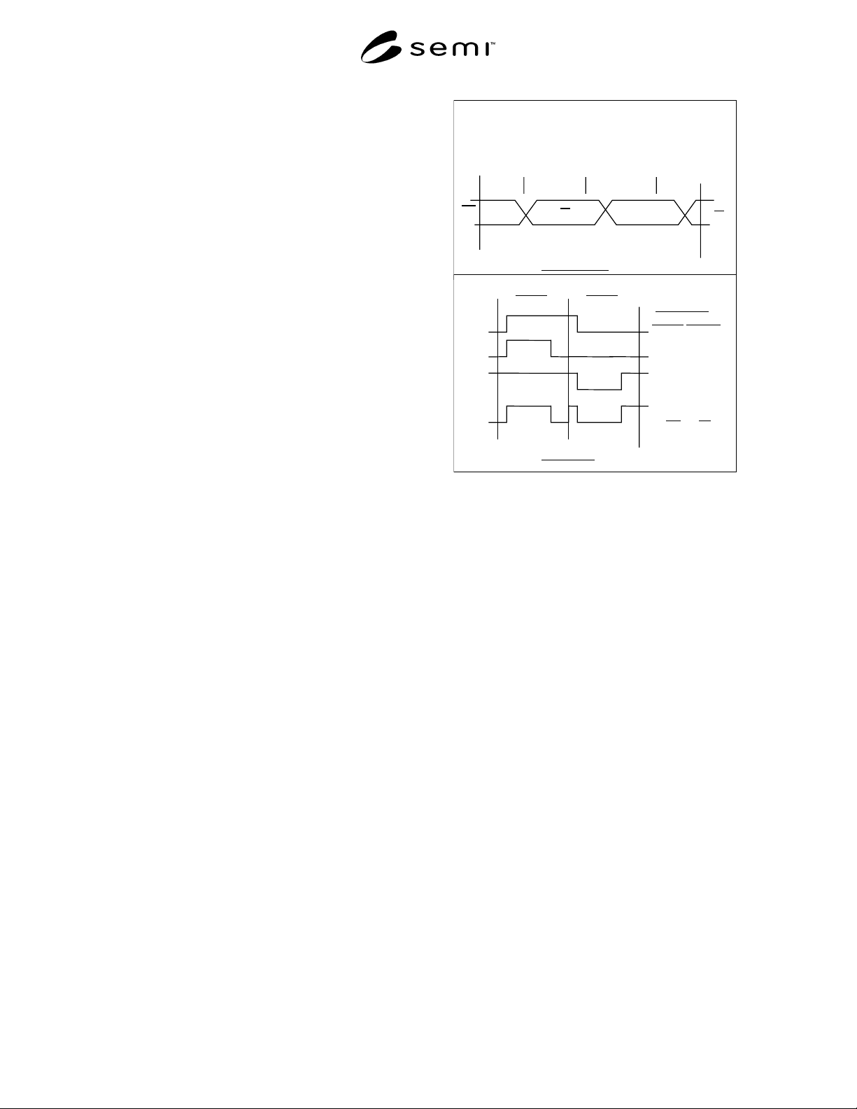
10.3.2 For clarification all drive edges are detected in
parallel in pairs. The intention is to sweep the compare
edge and detect the earliest occurrence of a drive edge
with the latest compare edge, as well as detect the latest
occurrence of a drive edge with the earliest compare
edge.
SBC Example
For pulse width = 33.3% (SBC
format) all formats start at 25% of the
programmed test cycle.
25% 33% 33%
25% 50% 75% 100% 0
DD
D
D
Data 1 Data 0
N
R
RTZ
RTO
SBC
Transitions
Data 1 Data 0
1 1
2 0
0 2
3
3
total: 6 6
Transitions
Figure 2
SBC Example and Transitions
10.3.3 The following Test Cycle Example and nested
loop outline describes the test flow:
for amplitude = 1V, 3V, 5V
for direction =
odd_pins_drive_&_even_pins_compare to
even_pins_drive_&_odd_pins_compare
for test_cycle = min_cycle to [min_cycle +
500*cycle_resolution] by
cycle_resolution, 3x min_cycle, 10x min cycle
for pulse width = 50% (RTZ/RTO formats)
= 33.3% (SBC format)
= don't care (NR format)
for format = NR, RTZ, RTO, SBC (NOTE 1: all
formats start at 25% of the programmed test
cycle)
for all format transitions (pattern data 0 and 1)
detect earliest occurrence of format
transition midpoint with the latest
compare pin
detect latest occurrence of format transition
midpoint with the earliest compare pin
error = (latest occurrence - earliest
occurrence)
end transitions
end format
end pulse width
end test_cycle
end direction
end amplitude
SEMI G80-0200 © SEMI 2000 6
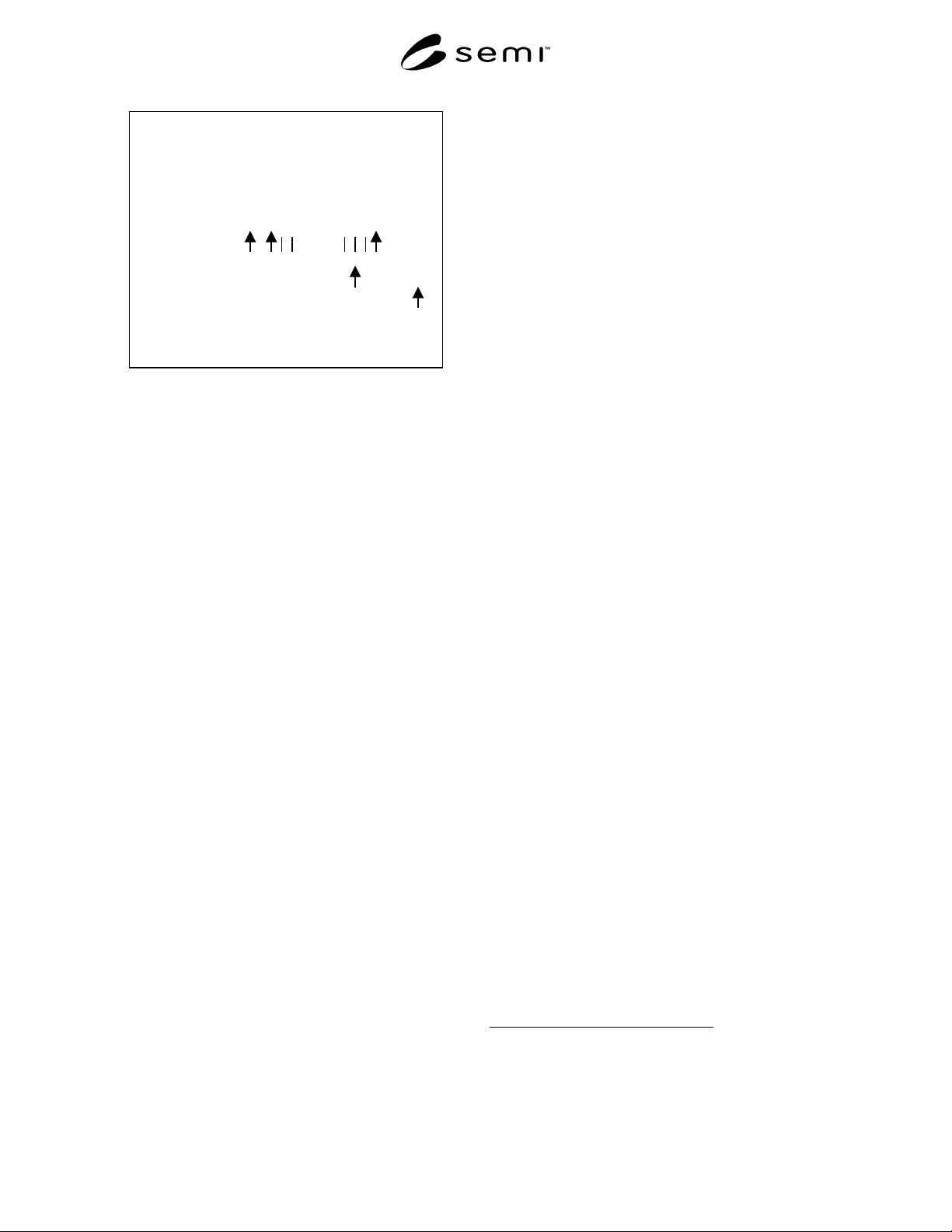
0 10ns 35ns
• 1 cycle: 3X = 30ns
•
1 cycle: 10X = 100ns
Total of 503 cycles. The intention of the last two cycles is
to define a period that is far beyond the minimum period.
Period resolution: 50ps
Minimum Period Cycle: 10ns
10ns to (10ns + 25ns) by 50ps
•
501 cycles:
For test_cycle = min_cycle to [min_cycle + 500*cycle
resolution] by cycle_resolution, 3Xmin_cycle, 10x min_cycle.
30ns
100ns
Example:
Figure 3
Test Cycle Example
10.3.4 Extended Delay Test — This test is used to
establish drive input to compare output timing accuracy
when timing generator delay values are programmed
beyond the length of the test cycle. Driver input delays
are programmed to occur in subsequent test cycles and
detected with compare delays originating in the corres-
ponding subsequent test cycle. The intention is the
same as Section 10.3.1 with the exception that edges
are programmed into a subsequent cycle. Conditions
such as formats and voltages have been reduced to keep
the amount of data collected down to a reasonable level.
10.3.4.1 The following nested loop outline describes
the test flow:
for amplitude = 3V
for direction =
odd_pins_drive_&_even_pins_compare to
even_pins_drive_&_odd_pins_compare
for test_cycle = min to 10*min by 0.1*min
for format = NR
for format_delay = test_cycle to max_delay by
0.25*test_cycle (max delay is beyond the cycle
boundary)
detect earliest occurrence of format
transition midpoint with the latest
compare pin using pattern expect
data shifted into the appropriate cycle
detect latest occurrence of format transition
midpoint with the earliest compare pin
using pattern expect data shifted into
the appropriate cycle
error = (latest occurrence - earliest
occurrence)
end delays
end format
end test cycles
end directions
end amplitude
10.3.5 Driver Z State Test — This test verifies the
timing accuracy of tester driver transitions from Z to
1/0 and from 1/0 to Z. Driver inputs are programmed to
transition to and from Z and 1/0 while being loaded
with 50 ohms terminated to drive 1 for Z to 0 and 0 to
Z, and 50 ohms terminated to drive 0 for Z to 1 and 1 to
Z
7
(reference load C). The following nested loop
outline describes the test flow:
for amplitude = 3V
for direction =
odd_pins_drive_&_even_pins_compare to
even_pins_drive_&_odd_pins_compare
for test_cycle = 5*min_cycle
for format_delay = 50%
for format = NR
detect earliest occurrence of Z to low tran-
sition at scaled midpoint with compare pins
detect latest occurrence of Z to low tran-
sition at scaled midpoint with compare pins
error=(latest occurrence - earliest occurrence)
detect earliest occurrence of Z to 1 tran-
sition at scaled midpoint with compare pins
detect latest occurrence of Z to 1 transition
at scaled midpoint with compare pins
error = (latest occurrence - earliest occur-
rence)
detect earliest occurrence of 0 to Z transition
at scaled midpoint with compare pins
detect latest occurrence of 0 to Z transition at
scaled midpoint with compare pins
error = (latest occurrence - earliest occur-
rence)
detect earliest occurrence of 1 to Z tran-
sition at scaled midpoint with compare pins
detect latest occurrence of 1 to Z transition
at scaled midpoint with compare pins
error = (latest occurrence - earliest occur-
rence)
end format
end format_delay
end test_cycle
end direction
end amplitude
10.3.6 Multiple Period Test
8
— This is an optional test
to be run only if the ATE supports dynamic (or “on-the-
fly”) time set switching. This test intention is similar
to Section 10.3.1 and 10.3.4 (timing linearity and
extended delay tests) except that the test period and
delay changes are generated dynamically within a
7 Tying two drivers together or connecting a resistor to a logic point is
acceptable. Note: Load “C”: 50 ohms to low for driver z to high and high to z
transitions. And 50 ohms to high for driver z to low and low to z transitions.
8 This algorithm requires 64 time sets. If the equipment does not have 64 time
sets, adjust the algorithm to accommodate the amount available and note the
differences on the exception page, Appendix 3.
SEMI G80-0200 © SEMI 20007
single test pattern burst. The following nested loop
outline describes the test flow:
for amplitude = 1V, 3V, 5V
for direction =
odd_pins_drive_&_even_pins_compare to
even_pins_drive_&_odd_pins_compare
execute single pattern with the following
dynamic changes:
Test
Cycle
Drive
Format
Format
Offset
Pulse
Width
Drive
Data
Compare
Offset
Expect
Data
min SBC 20% 33% 1 53% H
min SBC 20% 33% 1 86% L
min SBC 20% 33% 0 53% L
min SBC 20% 33% 0 86% H
min SBC 20% 33% 1 20% L
.
.
min SBC 20% 33% 0 20% H
64*min SBC 20% 33% 1 53% H
64*min SBC 20% 33% 1 86% L
64*min SBC 20% 33% 0 53% L
64*min SBC 20% 33% 0 86% H
64*min SBC 20% 33% 1 20% L
64*min SBC 20% 33% 0 20% H
2*min SBC 20% 33% 1 53% H
2*min SBC 20% 33% 1 86% L
2*min SBC 20% 33% 0 53% L
2*min SBC 20% 33% 0 86% H
2*min SBC 20% 33% 1 20% L
2*min SBC 20% 33% 0 20% H
63*min SBC 20% 33% 1 53% H
63*min SBC 20% 33% 1 86% L
63*min SBC 20% 33% 0 53% L
63*min SBC 20% 33% 0 86% H
63*min SBC 20% 33% 1 20% L
63*min SBC 20% 33% 0 20% H
.
.
32*min SBC 20% 33% 1 53% H
32*min SBC 20% 33% 1 86% L
32*min SBC 20% 33% 0 53% L
32*min SBC 20% 33% 0 86% H
32*min SBC 20% 33% 1 20% L
32*min SBC 20% 33% 0 20% H
detect earliest occurrence of format
transition midpoint with the latest
compare pin
detect latest occurrence of format transition
midpoint with the earliest compare pin
error = (latest occurrence - earliest occurrence)
end direction
end amplitude
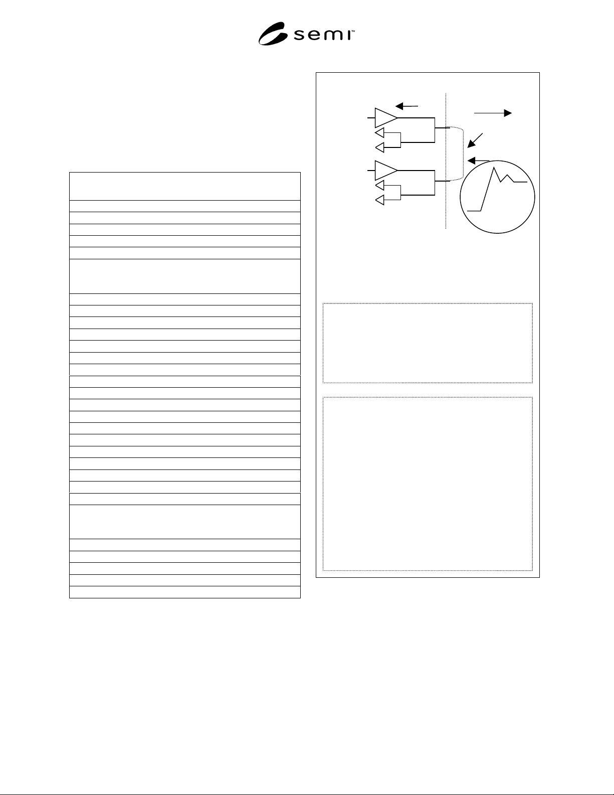
Pairs of adjacent tester pins can be shorted together
with a minimum length interconnect on the
performance board.
A reference for the oscilloscope measurement is
required. That reference can be any signal
synchronized to the test system's timing. The
reference signal chosen should be consistent and
stable. Examples of this may be another tester pin or
master oscillator reference signal.
Pin n
Driver
Receiver
Pin n+1
Driver
Receiver
N
OTE 1: The user of this method may find improved
driver signal attributes using an open circuit
performance board, versus the shorted board
indicated here for Level 2 Drive Input Timing Error
data collection. On the other hand the shorted
performance board, using the driver as the signal
source, is a viable approach for the Compare Output
Timing Error Test. Regardless, the user may
optionally choose to use a pulse generator as the
signal source for the Compare Output Timing Error
test. The 50-ohm pulse generator must have edge
speeds that are comparable to the driver it is
replacing. Test setup conditions and the pulse
generator rise time employed must be documented on
the exception page (Appendix 3).
Oscilloscope
Short (See
N
OTE 1.)
Tester
Performance
board
Figure 4
Level 2 Verification
10.4 Level 2 Tests — The efficiency of data collection
with Level 1 tests may preclude isolation of certain
specification components. The self-analysis procedures
may also mask some error terms that contribute to other
specification components. Therefore, Level 2 modules
are intended to supplement Level 1 results by using
external instruments to distinguish individual
specification components and provide detailed analysis