semi合集-English.pdf - 第6566页
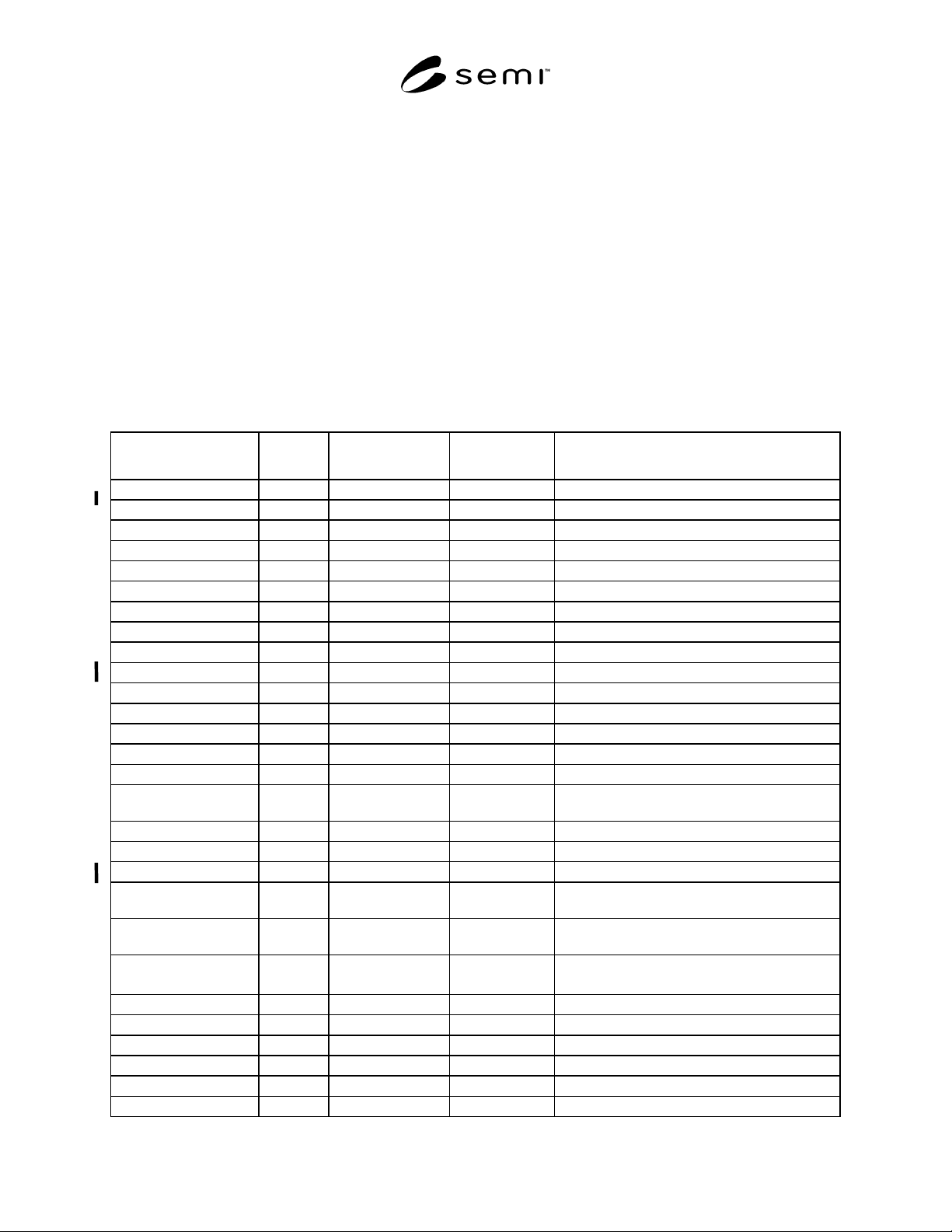
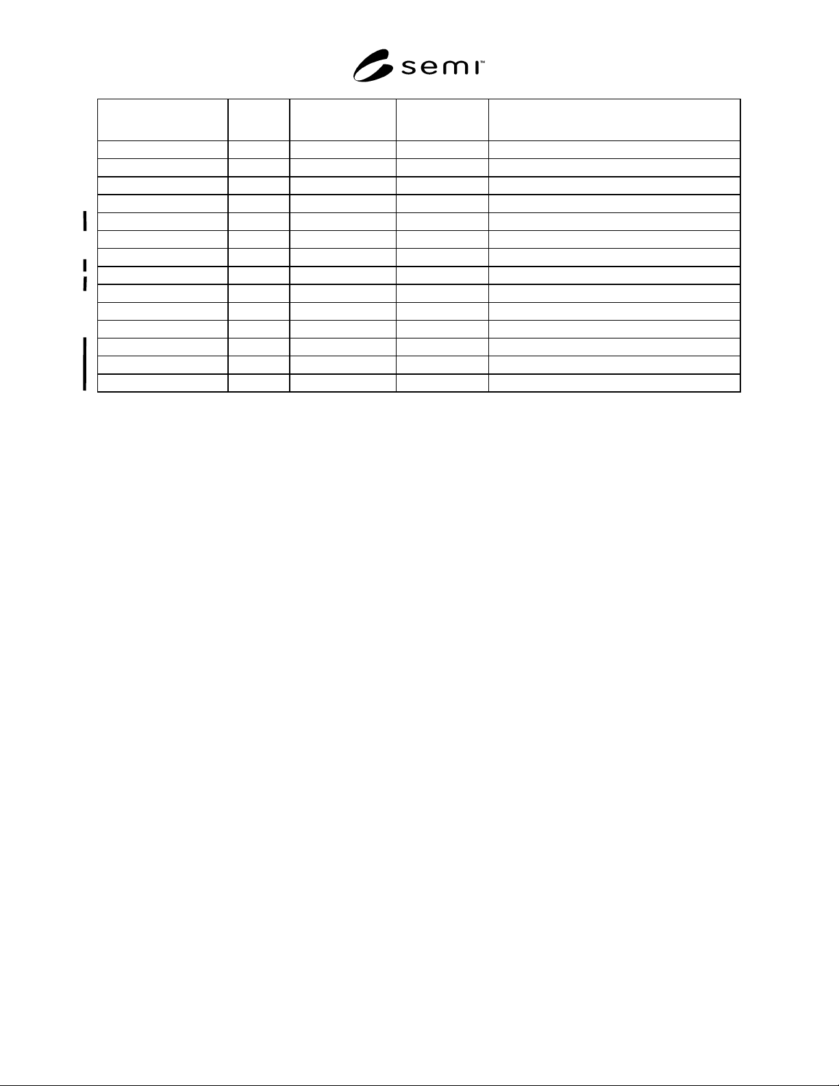
SEMI G85-0703 © SEMI 2001, 2003 4 Name Item or Attribute Defined In Mandatory or Optional Default Value BinQuality Attribute Map Data Items Optional “” BinDescription Attribute Map Data Items Optional “” FrameId Attribut…
SEMI G85-0703 © SEMI 2001, 2003 3
might be used for example to represent versions of the
map after each process step.
7.6.4 The Row items are defined as XML CDATA
section. The example below shows the Data item for a
binary map with two rows and two columns.
<Data>
<Row><! [CDATA[FFFF]]></Row>
<Row><! [CDATA[FF14]]></Row>
</Data>
7.6.4.1 A CDATA section contains data that should not
be parsed by the XML parser. After <! [CDATA[, only
the string ]]> will be interpreted by the XML parser. If
this string occurs in the actual data (for example in an
ASCII map) then it must be replaced by the string
]]> so that the XML parser will not interpret it as the
end of the CDATA section.
7.6.4.2 Each Row item specifies the BinCode for each
column in the row in a format that depends on the
BinType attribute.
7.6.4.3 The Row items must match the actual rows on
the substrate being mapped. The first row is the
topmost row as viewed with the substrate oriented
according to the value of Orientation.
7.6.4.4 The number of Row items must match the
Rows attribute if specified.
7.6.4.5 The number of columns in each Row item must
match the Columns attribute if specified.
Table 1 Items and Attributes Used
Name Item or
Attribute
Defined In Mandatory or
Optional
Default Value
xmlns Attribute Map Data Format Mandatory Must be “http://www.semi.org”
NullBin Attribute Map Data Items Mandatory No default
Map Item Map Data Format Mandatory No default
Device Item Map Data Format Mandatory No default
Data Item Map Data Format Mandatory No default
Row Item Map Data Format Mandatory No default
FormatRevision Attribute Map Data Items Optional Latest version of this standard
ProductId Attribute Map Data Items Optional “”
LotId Attribute Map Data Items Optional “”
Orientation Attribute Map Data Items Mandatory 0
WaferSize Attribute Map Data Items Optional 0
DeviceSizeX Attribute Map Data Items Optional 0
DeviceSizeY Attribute Map Data Items Optional 0
StepSizeX Attribute Map Data Items Optional 0
StepSizeY Attribute Map Data Items Optional 0
CassetteId
MagazineId
Attribute Map Data Items Optional “”
Rows Attribute Map Data Items Optional Can be derived from number of Row items
Columns Attribute Map Data Items Optional Can be derived from Row items
BinType (See Note 3.) Attribute Map Data Items Mandatory “ASCII”
ReferenceDevice Item Map Data Format Mandatory
(See Note 1.)
No default
ReferenceDeviceX Attribute Map Data Items Mandatory
(See Note 1.)
No default
ReferenceDeviceY Attribute Map Data Items Mandatory
(see Note 1)
No default
RefDevicePosX Attribute Map Data Items Optional 0.0
RefDevicePosY Attribute Map Data Items Optional 0.0
MapName Attribute Map Data Items Optional “”
MapVersion Attribute Map Data Items Optional “”
BinCode Attribute Map Data Items Optional 0
BinCount Attribute Map Data Items Optional 0
SEMI G85-0703 © SEMI 2001, 2003 4
Name Item or
Attribute
Defined In Mandatory or
Optional
Default Value
BinQuality Attribute Map Data Items Optional “”
BinDescription Attribute Map Data Items Optional “”
FrameId Attribute Map Data Items Optional “”
SupplierName Attribute Map Data Items Optional “”
OriginLocation Attribute Map Data Items Mandatory 0 (Center topside)
CreateDate Attribute Map Data Items Optional “”
Status Attribute Map Data Items Optional “”
Bin Item Map Data Format Optional No default
SlotNumber Attribute Map Data Items Optional 0
SubstrateNumber Attribute Map Data Items Optional 0
GoodDevices Attribute Map Data Items Optional 0
SubstrateType Attribute Map Data Items Mandatory
SubstrateId Attribute Map Data Items Mandatory
LastModified Attribute Map Data Items Optional
NOTE 1: There must be at least one ReferenceDevice item containing the ReferenceDeviceX and ReferenceDeviceY attributes.
NOTE 2: A substrate must have one and only one of these identifiers depending on the substrate type.
NOTE 3: Since XML is an ASCII only format BinType may only take the ASCII representation values “ASCII”, “Decimal”, “HexaDecimal”,
and not “Binary”.
SEMI G85-0703 © SEMI 2001, 2003 5
APPENDIX 1
EXAMPLE MAP DATA FILES
2
NOTICE: The material in this appendix is an official part of SEMI G85 and was approved by full letter ballot procedures on
March 12, 2003.
2 These examples are for a wafer map identified by WaferId. Other substrate types may also be represented. See Table 1.
A1-1 Simple ASCII Wafer Map
A1.1 This example illustrates the simplest possible
wafer map. It uses ASCII bin codes and contains only
the required data items.
<? xml version=" 1.0" ? >
<Map xmlns: " http://www.semi.org"
SubstrateType=" Wafer"
SubstrateId=" ZSDGS88DF" >
<Device
Orientation=" 0"
BinType=" Ascii"
NullBin=" "
OriginLocation=" 1" >
<Data >
<Row><! [CDATA[ 2C ]]></Row>
<Row><! [CDATA[ ~ 2C2 ]]></Row>
<Row><! [CDATA[222A1~ ]]></Row>
<Row><! [CDATA[21~ C22]]></Row>
<Row><! [CDATA[ ~ 2C2 ]]></Row>
<Row><! [CDATA[ 2C ]]></Row>
</Data>
</Device>
</Map>
A1-2 Detailed Binary Wafer Map
A1-2.1 The example below illustrates the use of binary
bin codes and contains not only the required data items,
but also some data items provided by the supplier.
<? xml version=" 1.0" ? >
<Map xmlns: " http://www.semi.org"
SubstrateType=" Wafer"
SubstrateId =" ZSDGS88DF"
FormatRevision=" SEMI G85-0703" >
<Device
ProductId=" 854CS1C"
LotId=" wksfd87dcj37"
Orientation=" 0"
DeviceSizeX=" 343.8"
DeviceSizeY=" 373.1"
Rows=" 6"
Columns=" 6"
BinType=" HexaDecimal"
FrameId=" KJKSDFK45"
NullBin=" FF"
SupplierName=" Company X"
OriginLocation=" 1"
CreateDate=" 2002110112000000"
LastModified=" 2003010612000000"
Status=" Product" >
<ReferenceDevice
ReferenceDeviceX=" 2"
ReferenceDeviceY=" -3"
RefDevicePosX=" 2"
RefDevicePosY=" 2"
/>
<ReferenceDevice
ReferenceDeviceX=" 4"
ReferenceDeviceY=" -5"
RefDevicePosX=" 2"
RefDevicePosY=" 2"
/>
<Bin
BinCode=" 02"
BinQuality=" Pass"
BinDescription=" 500MHz"
/>
<Data MapName=" SortGrade" MapVersion=" 1" >