semi合集-English.pdf - 第6572页
SEMI G86-0303 © SEMI 2003 4 NOTICE: SEMI makes no warranties or representations as to the suitability o f the standards set forth herei n for any pa rticular application. The determination of the suitability o f the stan…
SEMI G86-0303 © SEMI 2003 3
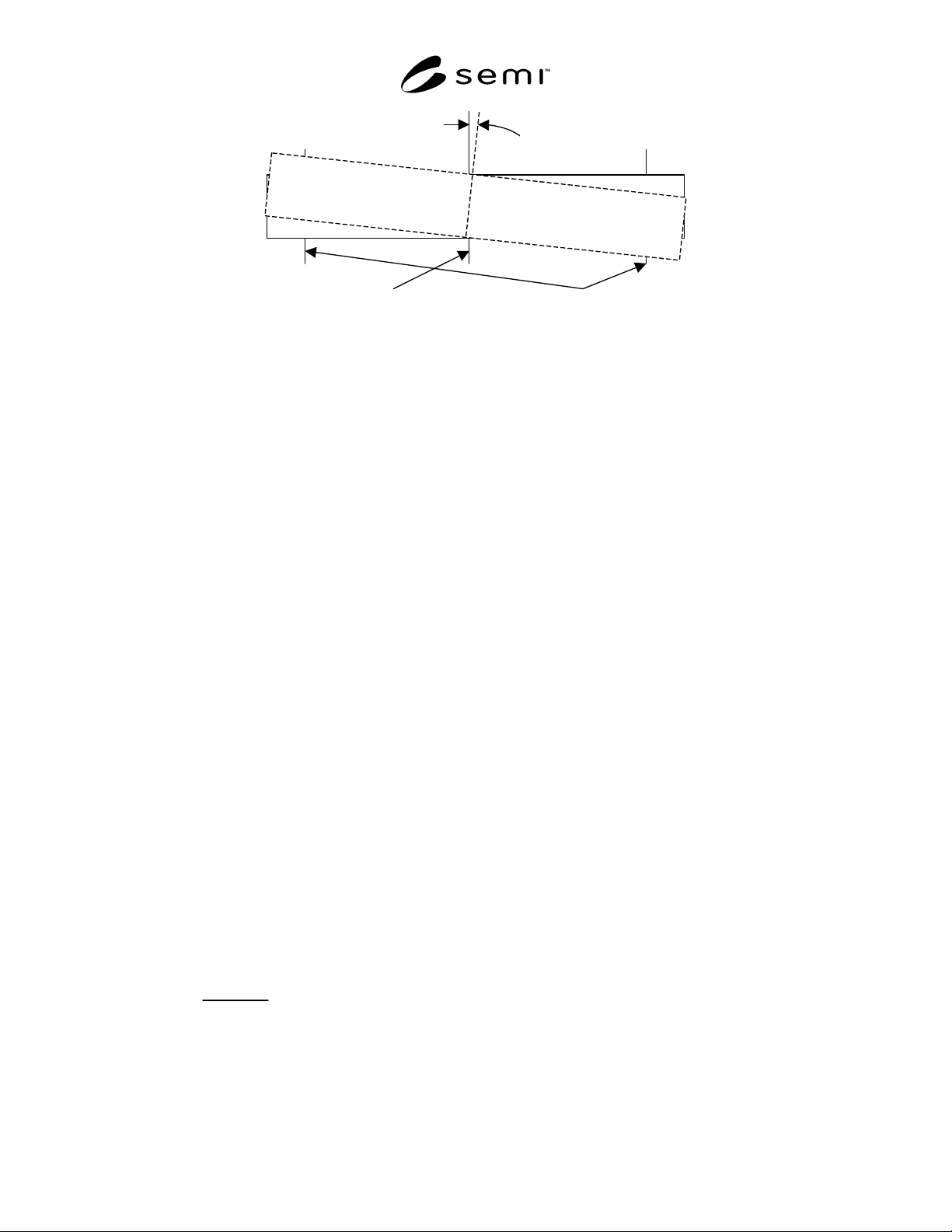
Datum plane Support
5 °
Figure 3
Setting Condition of Test Specimen
7 Test Specimens
7.1 The shape and dimensions of the test specimens
shall be agreed between the interested parties.
7.2 Test specimen shall be Silicon Die.
7.3 At least 25 test specimens shall be pulled from a
wafer.
8 Procedure
8.1 Measure the thickness h, width b, and length w.
The accuracy of h and b shall be within ± 5%.
8.2 Adjust the span L in accordance with the following
conditions,
at h < 0.1 mm : L ≤ 2 mm and L ≤ 50 h
at h ≥ 0.1 mm : 2 mm ≤ L and L ≤ 20 h
8.3 Place the test specimen on the two supports within
± 5° of the deviation from datum plane (see Figure 3).
The evaluated surface shall be applied the tensile force.
8.4 Set the test speed less than 5 mm/min in order to
avoid the impact on test specimen and apply the force at
midspan.
8.5 Record the force of the specimen at the break.
9 Calculation
9.1 Flexural Stress — Calculate the flexural stress
parameters defined in Section 4 using the following
equation:
(1)
σ
fB
=
3
P
B
L
2
bh
2
Where:
σ
fB
is the flexural stress at break in question (Mpa);
P
B
is the applied force at break, in newtons (N);
L is the span, in millimeters (mm);
b is the width, in millimeters (mm), of the test
specimen; and
h is the thickness, in millimeters (mm), of the test
specimen.
NOTE 5: Equation (1) can only be used for test specimens
with linear stress/strain behavior.
10 Test Report
10.1 The test report shall include the following
information:
• the directions major axes of the specimens if test
specimen has,
• the evaluated surface,
• the dimensions of the test specimens (thickness h,
width b, length w),
• the nominal span length used,
• the number of specimens tested,
• the speed of testing,
• the individual test results, the flexural stress at
break, and
• the date of the test.
SEMI G86-0303 © SEMI 2003 4
NOTICE: SEMI makes no warranties or
representations as to the suitability of the standards set
forth herein for any particular application. The
determination of the suitability of the standard is solely
the responsibility of the user. Users are cautioned to
refer to manufacturer's instructions, product labels,
product data sheets, and other relevant literature,
respecting any materials or equipment mentioned
herein. These standards are subject to change without
notice.
By publication of this standard, Semiconductor
Equipment and Materials International (SEMI) takes no
position respecting the validity of any patent rights or
copyrights asserted in connection with any items
mentioned in this standard. Users of this standard are
expressly advised that determination of any such patent
rights or copyrights, and the risk of infringement of
such rights are entirely their own responsibility.
SEMI G86-0303 © SEMI 2003 5
RELATED INFORMATION 1
ADDITIONAL INFORMATION FOR TESTING
NOTICE: This related information is not an official part of SEMI G86 and was derived from the work of the
originating task force. This related information was approved for publication by full letter ballot procedures on
January 10, 2003. It is provided for information purposes.
R1-1 Test Machine
R1-1.1 When the measurement of deflection is based
on the movement of loading edge, the frame
compliance of the test machine should be more than
40 kN/mm.
R1-1.2 The interval of data sampling, such as test force
and movement of the loading edge, should be more than
500 times per second when the test machine records the
data in digital format.
R1-2 Test Specimens
R1-2.1 The number of test specimen is 0.25 of
Acceptance Quality Level, specified in ISO/DIS2859-
1.2,Sampling procedures for inspection by attributes
— Part 1: Sampling schemes indexed by acceptable
quality level (AQL) for lot-by-lot inspection.
R1-2.2 Test specimens should be pulled from a wafer
in every direction without leaning.
R1-2.3 When test results are compared, same test
specimens size (span L and width b) should be used.
R1-2.4 When excessive film is attached to test
specimens, equation (1) in Section 9.1 for stress on a
silicon material may not be applied.
R1-3 Recording the Force
R1-3.1 Not only the force at the break points but also
test force of the specimen under the test should be
recorded. It is recommended that an automatic
recording system is used .
R1-4 Test Report
R1-4.1 Test report should include the failure
characteristics of the failed specimens.
R1-4.2 When possible, the test report should include
failures which occur at any notable defect on the die.
NOTICE: SEMI makes no warranties or
representations as to the suitability of the standards set
forth herein for any particular application. The
determination of the suitability of the standard is solely
the responsibility of the user. Users are cautioned to
refer to manufacturer's instructions, product labels,
product data sheets, and other relevant literature,
respecting any materials or equipment mentioned
herein. These standards are subject to change without
notice.
By publication of this standard, Semiconductor
Equipment and Materials International (SEMI) takes no
position respecting the validity of any patent rights or
copyrights asserted in connection with any items
mentioned in this standard. Users of this standard are
expressly advised that determination of any such patent
rights or copyrights, and the risk of infringement of
such rights are entirely their own responsibility.
Copyright by SEMI® (Semiconductor Equipment and Materials
International), 3081 Zanker Road, San Jose, CA 95134. Reproduction o
f
the contents in whole or in part is forbidden without express written
consent of SEMI.