semi合集-English.pdf - 第7217页
SEMI MF26-0305 © SEMI 2003, 2005 7 5.4.2 Etch the lapped surface as follows: 5.4.2.1 Etch germanium surfaces with germanium etchant solution (see ¶5.2.2) for 1 min at 25 C. 5.4.2.2 Etch silicon surfaces with 45% KOH so…
SEMI MF26-0305 © SEMI 2003, 2005 6
(
111
)
GERMANIUM
(110) GERMANIUM
(100) GERMANIUM
(100) SILICON
(110) SILICON
(111) SILICON
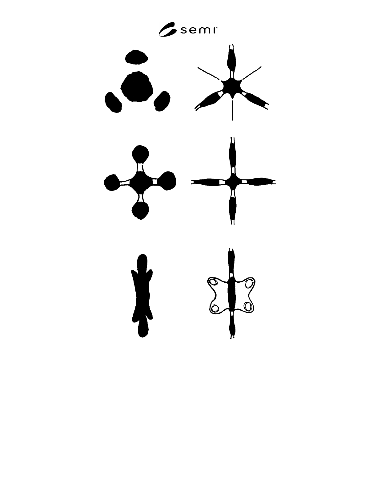
Figure 2
Optical Reflections from Etched Germanium and Silicon Surfaces
5.3.2 Stage — capable of rotation both vertically and horizontally and calibrated to permit measurements of
deviation from the 0° reference plane. Means shall be provided to securely position the reflecting surface of the
crystal on the stage of the apparatus.
5.4 Procedure
5.4.1 Abrade the specimen surface by lapping with No. 600 silicon carbide abrasive. The abrasive grain size
specified for this purpose shall comply with the appropriate specifications of ANSI B74.10. Care must be taken to
produce no angular deviation from the original surface during the lapping operation.

SEMI MF26-0305 © SEMI 2003, 2005 7
5.4.2 Etch the lapped surface as follows:
5.4.2.1 Etch germanium surfaces with germanium etchant solution (see ¶5.2.2) for 1 min at 25C.
5.4.2.2 Etch silicon surfaces with 45% KOH solution (see ¶5.2.5) or 50% NaOH solution (see ¶5.2.6) for 5 min at
65C.
5.4.3 Mount the specimen containing the prepared surface on the goniometer in the path of the incident light beam.
5.4.4 Adjust the position of the specimen surface to bring the center of the reflected light pattern to the zero
reference point described in ¶5.3.1. The angular reading on the goniometer required to make this adjustment is the
degree of misorientation on the surface under examination.
5.4.5
Check this measurement, where possible, by rotating the surface through 180° of arc. The angular deviation
must remain constant in magnitude but is opposite in sign.
5.4.6 Rotate the specimen through 90° of arc about a normal to the surface under investigation, and repeat the
procedure to measure the second component of angular deviation.
5.5 Calculations
5.5.1 Calculate and record the total angular deviation,
, in accordance with ¶4.5.2.
6 Report
6.1 Report the following information:
6.1.1 Method used (X-ray or optical),
6.1.2 Material investigated,
6.1.3 Crystal reference plane,
6.1.4 Deviation of prepared surface from this reference plane in two mutually perpendicular directions, and
6.1.5 Total angular deviation of prepared surface from the reference plane
7 Precision and Bias
7.1 Test Method A, X-ray Diffraction Orientation — The single instrument precision of the method as defined in
ASTM Practice E 177 is ±15 min of arc (3S) using commercially available X-ray equipment.
7.2 Test Method B, Optical Orientation — The single instrument precision of the method as defined in ASTM
Practice E 177 is ±30 min of arc (3S) using commercially available optical orientation equipment.
8 Keywords
germanium; orientation; preferential etch; semiconductor; silicon; X-ray diffraction
NOTICE: SEMI makes no warranties or representations as to the suitability of the standards set forth herein for any
particular application. The determination of the suitability of the standard is solely the responsibility of the user.
Users are cautioned to refer to manufacturer's instructions, product labels, product data sheets, and other relevant
literature, respecting any materials or equipment mentioned herein. These standards are subject to change without
notice.
By publication of this standard, Semiconductor Equipment and Materials International (SEMI) takes no position
respecting the validity of any patent rights or copyrights asserted in connection with any items mentioned in this
standard. Users of this standard are expressly advised that determination of any such patent rights or copyrights, and
the risk of infringement of such rights are entirely their own responsibility.
Copyright by SEMI® (Semiconductor Equipment and Materials
International), 3081 Zanker Road, San Jose, CA 95134. Reproduction of
the contents in whole or in part is forbidden without express written
consent of SEMI.

SEMI MF43-0705 © SEMI 2003, 2005 1
SEMI MF43-0705
TEST METHODS FOR RESISTIVITY OF SEMICONDUCTOR
MATERIALS
This test method was technically approved by the global Silicon Wafer Committee. This edition was
approved for publication by the global Audits and Reviews Subcommittee on April 7, 2005. It was available
at www.semi.org in June 2005 and on CD-ROM in July 2005. Original edition published by ASTM
International as ASTM F 43-64T. Last previous edition SEMI MF43-99.
1 Purpose
1.1 The resistivity of a semiconductor material is an important materials acceptance requirement. Resistivity
determinations made during device fabrication are also widely used for quality control purposes.
1.2 These test methods cover two procedures which are widely used for making routine measurements.
2 Scope
2.1 The two test methods in this standard are as follows:
2.1.1 Method A, Two-Probe — This test method requires a bar specimen of measurable cross section and with
cross-sectional dimensions small in comparison with the length of the bar. For materials for which no specific
referee method has been developed, this test method is recommended for materials acceptance purposes.
2.1.2 Method B, Four-Probe — This test method is rapid and does not require a specimen of regular cross section.
This test method may be used on irregularly shaped specimens, provided a flat region is available for the contacting
probes. As described in this standard, this test method is applicable only to specimens such that the thickness of the
specimen and the distance from any probe point to the nearest edge are both at least four times the probe spacing.
For the special case of specimens of circular cross section with thickness more than one, but less than four, times the
probe spacing, measurements by this test method are possible; the required application of approximate geometric
corrections results in improved accuracy (see ¶10.1.3).
2.2 In general, resistivity measurements are most reliable when made on single crystals, since with such material
local variations in impurity which affect the resistivity are less severe. Localized impurity segregation at grain
boundaries in polycrystalline material may result in large resistivity variations. Such effects are common to either of
the measurement test methods but are more severe with the four-probe test method, and its use, therefore, is not
recommended for polycrystalline material.
2.3 The values stated in SI units are to be regarded as the standard. The values given in parentheses are for
information only.
NOTE 1: DIN 50430 is an equivalent method to Method A and DIN 50431 is an equivalent method to Method B.
NOTE 2: Other standardized test methods are preferred for use in various special circumstances. For measurements on thin
wafers, use SEMI MF84; this method is preferred for referee measurements on silicon wafers. For measurements on specimens
for which point contacts are unsatisfactory, use a procedure in ASTM Test Methods F 76 based either on Van Der Pauw or bridge
specimens. For two-probe referee measurements on cylindrical single crystal bars, use SEMI MF397. For four-probe referee
measurements of sheet resistance on epitaxial layers deposited on or diffused or implanted into opposite conductivity-type
substrates, use SEMI MF374.
NOTICE: This standard does not purport to address safety issues, if any, associated with its use. It is the
responsibility of the user of this standard to establish appropriate safety and health guides and determine the
applicability of regulatory or other limitations prior to use.
3 Limitations
3.1 In making resistivity measurements, spurious results can arise from a number of sources. The following must
be guarded against: