semi合集-English.pdf - 第7224页
SEMI MF43-0705 © SEMI 2003, 2005 7 r = resistivity for reverse curre nt, ·cm, V r = potential drop across the two inner probes for reverse c u rrent, V, and I r = reverse curre nt, A. 10.1.3 For specimens of circular…

SEMI MF43-0705 © SEMI 2003, 2005 6
9.2.3 Measure the potential, first across the standard resistance, then across the potential probes, and again across
the standard resistance. During the measurement, the potential across the standard resistance shall not change by
more than 0.5%.
9.2.4 Reverse the direction of the current and repeat the procedure of ¶9.2.3.
9.2.5 If desired, move the probes to a new location on the specimen and repeat the measurements.
9.3 Four-Probe Method
9.3.1 Lower the probes onto the abraded surface of the specimen at a location such that the distance from each
probe to the nearest edge is at least four times the probe spacing, pass a known current through the outer probes, and
measure the potential drop across the inner probes.
NOTE 10: The current should be of sufficient magnitude that the potential drop can be measured to the required precision. If the
current is chosen equal to 2 times the probe spacing, the potential drop across the inner probes for measurements on semi-
infinite solids is numerically equal to the resistivity and calculations may be avoided.
9.3.2 Reverse the direction of the current and repeat the measurement.
10 Calculations
10.1 Calculate the resistivity for both forward and reverse current directions:
10.1.1 Two-Probe Test Method
fsfs
f
s
f
VV
V
L
AR
21
2
and
rsrs
r
s
r
VV
V
L
AR
21
2
(4)
where:
f
=
resistivity for forward current, ·cm,
R
s
=
resistance of standard resistor, ,
A = cross-sectional area normal to the current, cm
2
,
L = distance between the two probes, cm,
V
f
= potential drop across the two probes for forward current, V,
V
s1f
= first voltage across standard resistor for forward current, V,
V
s2f
= second voltage across standard resistor for forward current, V,
r
=
resistivity for reverse current, ·cm,
V
r
= potential drop across the two probes for reverse current, V,
V
s1r
= voltage across standard resistor for reverse current, V, and
V
s2r
= second voltage across standard resistor for reverse current, V.
10.1.2 Four-Probe Method
f
f
f
I
V
s
2 and
r
r
r
I
V
s
2 (5)
where:
f
=
resistivity for forward current, ·cm,
s = spacing between adjacent probes, cm,
V
f
= potential drop across the two inner probes for forward current, V,
I
f
= forward current, A,
SEMI MF43-0705 © SEMI 2003, 2005 7
r
=
resistivity for reverse current, ·cm,
V
r
= potential drop across the two inner probes for reverse current, V, and
I
r
= reverse current, A.
10.1.3 For specimens of circular cross section with thickness more than one, but less than four, times the probe
spacing (that is, the distance between adjacent points of the four-probe array being used), calculate the ratio of
average specimen thickness, w, to average probe spacing,
,s and the ratio of average probe spacing, ,s to average
specimen diameter, D, and proceed as follows:
10.1.3.1 For specimens for which the ratio of thickness to probe spacing is in the range
:5.21
s
w
f
f
f
I
V
wF
s
w
F
2
and
r
r
r
I
V
wF
s
w
F
2
(6)
10.1.3.2 For specimens for which the ratio of thickness to probe spacing is in the range
:45.2
s
w
f
f
f
I
V
w
s
w
F
532.4
and
r
r
r
I
V
w
s
w
F
532.4
(7)
where
s
w
F
and F
2
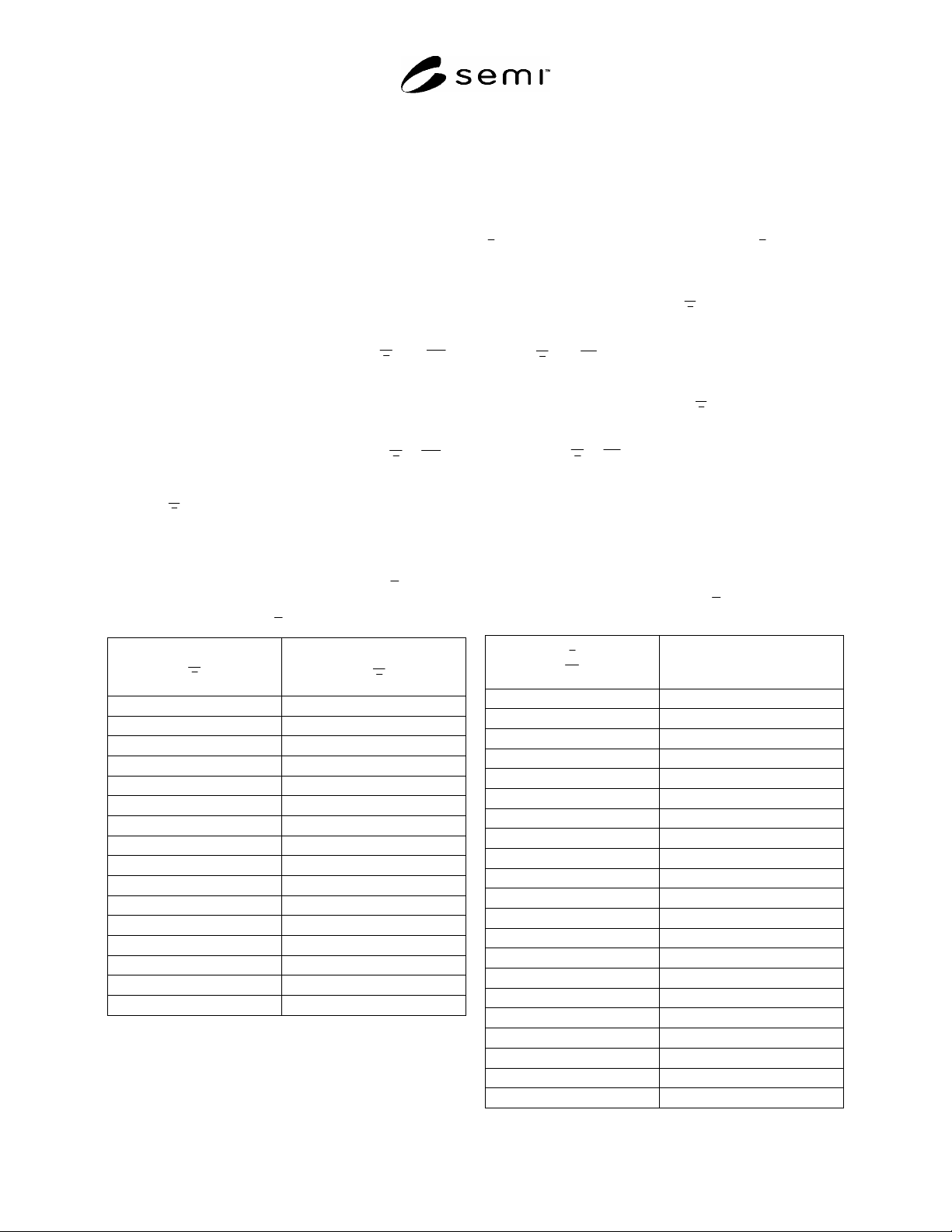
are given in Tables 1 and 2, respectively.
NOTE 11: These geometric correction factors are approximate but are valid within 2% if the specimen diameter is greater than
25.4 mm (1 in.). For smaller diameter specimens, the factors are of unknown accuracy.
Table 1 Thickness Correction Factor,
)sF(w/ , as a
Function of the Ratio of Wafer Thickness, w, to
Average Probe Spacing,
.s
s
w
s
w
F
1.0 0.921
1.2 0.864
1.4 0.803
1.6 0.742
1.8 0.685
2.0 0.634
2.2 0.587
2.4 0.546
2.6 0.510
2.8 0.477
3.0 0.448
3.2 0.422
3.4 0.399
3.6 0.378
3.8 0.359
4.0 0.342
Table 2 Correction Factor, F
2
, as a Function of the
Ratio of Average Probe Spacing,
,s
to Wafer
Diameter, D
D
s
F
2
0 4.532
0.005 4.531
0.010 4.528
0.015 4.524
0.020 4.517
0.025 4.508
0.030 4.497
0.035 4.485
0.040 4.470
0.045 4.454
0.050 4.436
0.055 4.417
0.060 4.395
0.065 4.372
0.070 4.348
0.075 4.322
0.080 4.294
0.085 4.265
0.090 4.235
0.095 4.204
0.100 4.171

SEMI MF43-0705 © SEMI 2003, 2005 8
10.2 Calculate the average resistivity at the temperature of measurement as follows:
2
rf
av
(8)
10.3 If necessary, correct the resistivity to a reference temperature of 23C as follows:
)( 231
23
TC
T
av
(9)
where:
23
= resistivity corrected to 23C, ·cm,
av
= average resistivity at temperature of measurement, ·cm,
C
T
= temperature coefficient appropriate to specimen (see ¶3.1.4 and Note 3), and
T = temperature of measurement, °C.
NOTE 12: The temperature coefficients of resistivity cited here for germanium and silicon are valid for measurements taken in
range from 18 to 28°C.
NOTE 13: If desired, correction may be made for probes with unequal probe spacings by multiplying the average resistivity by
the probe spacing correction factor (F
sp
) (see Note 4) before correcting the resistivity to the reference temperature.
11 Report
11.1 For referee tests, report the following information:
11.1.1 Identification of test specimen,
11.1.2 Ambient temperature of test,
11.1.3 Probe spacing,
11.1.4 Method of determining cross-sectional area,
11.1.5 Method of surface preparation,
11.1.6 Instrumentation used to measure current and voltage,
11.1.7 Location of measurement in relation to a reference point on the specimen,
11.1.8 Magnitude of current,
11.1.9 Calculated resistivity for both current directions, and
11.1.10 Average resistivity at measurement temperature, and if computed, at 23C.
11.2 For routine tests, report the items in ¶¶11.1.1, 11.1.2, and 11.1.10 together with such other items listed above
as may be deemed significant.
12 Precision
12.1 Silicon bars and wafers with resistivity in the range from 5 to 20 ·cm were tested in a nine-laboratory round
robin conducted in 1965. No geometrical or temperature correction factors were applied. The multilaboratory
precisions, as estimated from three times the mean values of the relative sample standard deviations, were ±6% for
the two-probe test method (on bars) and ±8% for the four-probe test method (on wafers). The precision for other
resistivity ranges and other materials has not been established.
13 Keywords
13.1 germanium; resistivity; semiconductor; silicon