semi合集-English.pdf - 第7237页
SEMI MF154-0305 © SEMI 2003, 2005 11 NOTICE: SEMI makes no warranties or represen tations as to the suitability o f the standards set forth herein for any particular application. The determination of the suitability of t…
SEMI MF154-0305 © SEMI 2003, 2005 10
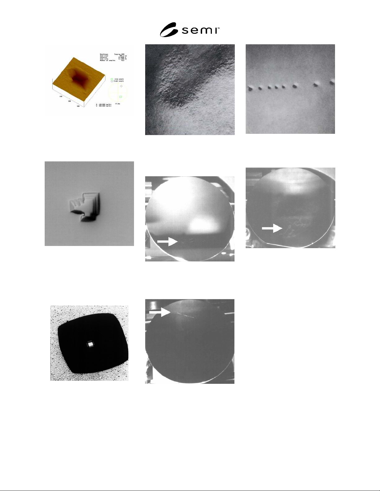
Figure 61
Atomic Force Microscope (AFM)
Image of a Faceted COP
Figure 62
Pit (Usually Associated With
Insufficient Polishing of Caustic
Etched Wafer),
Magnification 1000×
NOTE: Air Pocket Size Ranges from a
Few Micrometers to a Few Hundred
Micrometers
Figure 63
Pit Associated with a Crystal Air
Pocket on Lapped Wafer
Figure 64
Saw Blade Defect Seen on
Lapped and Etched Wafer,
Magnification 6×
Figure 65
Multiple Scratches Located by
the Arrow under High Intensity
Light, Full Wafer View
Figure 66
A Single Long Arc Scratch
Located by the Arrow
Under High Intensity Light,
Full Wafer View
Figure 67
Scratch Resulting in a Series of
Pits Following Chemical Etching,
Magnification 70×
Figure 68
Stains from Improper Cleaning
or Drying Located by the Arrow
under High Intensity Light,
Full Wafer View

SEMI MF154-0305 © SEMI 2003, 2005 11
NOTICE: SEMI makes no warranties or representations as to the suitability of the standards set forth herein for any
particular application. The determination of the suitability of the standard is solely the responsibility of the user.
Users are cautioned to refer to manufacturer's instructions, product labels, product data sheets, and other relevant
literature, respecting any materials or equipment mentioned herein. These standards are subject to change without
notice.
By publication of this standard, Semiconductor Equipment and Materials International (SEMI) takes no position
respecting the validity of any patent rights or copyrights asserted in connection with any items mentioned in this
standard. Users of this standard are expressly advised that determination of any such patent rights or copyrights, and
the risk of infringement of such rights are entirely their own responsibility.
Copyright by SEMI® (Semiconductor Equipment and Materials
International), 3081 Zanker Road, San Jose, CA 95134. Reproduction of
the contents in whole or in part is forbidden without express written
consent of SEMI.

SEMI MF525-0705 © SEMI 2003, 2005 1
SEMI MF525-0705
TEST METHOD FOR MEASURING RESISTIVITY OF SILICON WAFERS
USING A SPREADING RESISTANCE PROBE
This standard was technically approved by the global Silicon Wafer Committee. This edition was approved
for publication by the global Audits and Reviews Subcommittee on April 7, 2005. It was available at
www.semi.org in June 2005 and on CD-ROM in July 2005. Original edition published by ASTM
International as ASTM F 525-77T. Last previous edition SEMI MF525-00a.
1 Purpose
1.1 This test method provides means for directly determining the resistivity of a substrate or of an epitaxial layer of
thickness greater than 20 times the effective electrical contact radius. Unlike SEMI MF84, SEMI MF374, and
SEMI MF1392, it can provide lateral spatial resolution of resistivity on the order of a few micrometers.
1.2 This test method is intended primarily for use in process control, research, and development applications. In
the absence of between-laboratory precision data, this test method is not recommended for use between supplier and
customer unless correlation experiments have been conducted between the parties.
2 Scope
2.1 This test method covers the measurement of the resistivity of a silicon substrate of known orientation and type,
or of a uniform silicon epitaxial layer of known orientation and type that is deposited on a substrate of the same or
opposite type. Resistivity of the epitaxial films can be evaluated without the necessity of thin film correction factors
provided that the ratio of layer thickness to effective probe contact radius is greater than 20.
2.2 This test method is comparative in that the resistivity of an unknown specimen is determined by comparing its
measured spreading resistance with that of calibration standards of known resistivity. These calibration standards
must have the same surface finish, conductivity type, and orientation as the unknown specimen.
2.3 This test method is intended for use on silicon substrates and epitaxial layers. Within-laboratory precision has
been determined through a multilaboratory experiment on substrates having resistivities from 0.01 to 200 ·cm.
2.3.1 The principles of this test method can be extended to lower and higher specimen resistivity values, but the
precision of the test method has not been evaluated for values other than those in the range given in ¶2.3.
2.4 This test method is nondestructive in the sense that the specimen is not totally destroyed in making the
measurements, the specimen need not be cut into a special shape, and no destructive processing need be done on the
specimen. However, the probe can produce mechanical damage that may be detrimental to a device fabricated in the
probed area.
2.5 The volume of semiconductor material sampled is proportional to the third power of the effective electrical
contact radius of the probe. For an effective electrical contact radius of 2 m, the volume sampled by a single probe
is approximately 10
11
cm
3
.
NOTICE: This standard does not purport to address safety issues, if any, associated with its use. It is the
responsibility of the user of this standard to establish appropriate safety and health guides and determine the
applicability of regulatory or other limitations prior to use.
3 Limitations
3.1 Temperature — Spreading resistance measurements are sensitive to the temperature of the specimen.
Therefore, it is important that the calibration and actual measurements be made at the same temperature.
3.2 Light — Photoconductive and photovoltaic effects can seriously influence the resistance determined by this test
method, especially on wafers with p-n junctions. All determinations shall be made in a dark chamber, or if
experience shows that the material is insensitive to illumination of this type, in diffuse room light.