semi合集-English.pdf - 第7246页
SEMI MF525-0705 © SEMI 2003, 2005 9 where: R 0 = resistance of the standard resistor, , and log( i 1 / i 2 ) = output of t he log com parator. 14.2 Calculate and record the m ean value of the spreading resistance of ea…

SEMI MF525-0705 © SEMI 2003, 2005 8
13 Procedure
13.1 Handle the specimen carefully to avoid contamination or damage to the surface.
13.2 Make all measurements with an ambient temperature of 23 ± 3°C. Record the ambient temperature.
13.3 Determine the orientation of the specimen surface in accordance with SEMI MF26, determine the
conductivity type of the substrate and, if present, the epitaxial layer in accordance with SEMI MF42. For epitaxial
layers, determine the thickness in accordance with either SEMI MF95 or SEMI MF110. Record the results.
13.4 Prepare all bulk specimens to be tested using the same procedure as was used for the calibration specimens in
¶12.2. Do not prepare the surface of any epitaxial specimens. Thoroughly clean polishing material residues from
the specimen using water or solvent as necessary. If the materials of ¶8.4.1 or ¶8.4.3 were used for specimen
preparation, proceed to ¶13.5, otherwise proceed to ¶13.6.
13.5 Place the specimen on a hot plate with the surface to be measured upwards, not in contact with the hot plate.
Heat the specimen in air at 140 ± 20°C for 10 to 15 min. Remove the specimen from the hot plate. Allow the
specimen to return to 23 ± 3°C before continuing with the measurements.
13.6 Rigidly mount specimen on stage under probes. Use of wax mounting to base block used to hold specimen
during surface preparation or use of vacuum clamping is acceptable. Position the specimen on the specimen holder
so that the probe or probes will be applied at the desired measurement location.
13.7 Lower the points to make contact with the specimen surface, and adjust to within 0.1% (unless the comparator
method is being used) the voltage or current source to the desired value (see ¶11.8).
13.8 After a stabilization period of 1 s or longer, measure and record the current in milliamperes as I (constant-
voltage method), the voltage in millivolts as V (constant-current method), or the output of the log comparator as
log(i
1
/i
2
) (log comparator method).
13.9 Adjust the voltage source to a value of 20 mV or less or short circuit the current source and lift the probes.
13.10 Move the specimen to the next position, making sure that the step spacing is larger than the diameter of the
specimen area damaged by the probes.
13.11 Note and record the step spacing.
13.12 Repeat ¶¶13.6 through 13.11 until the desired number of measurements has been made.
14 Calculations
14.1 Calculate the spreading resistance, R
s
, in ohms, for each measurement as follows:
14.1.1 Constant-Voltage Method
I
V
R
s
(3)
where:
V
= applied voltage, mV, and
I = measured current, mA.
14.1.2 Constant-Current Method
I
V
R
s
(4)
where:
V
= measured voltage, mV, and
I = applied current, mA.
14.1.3 Comparator Method
)/log(
210
iiRR
s
(5)

SEMI MF525-0705 © SEMI 2003, 2005 9
where:
R
0
=
resistance of the standard resistor, , and
log(i
1
/i
2
) = output of the log comparator.
14.2 Calculate and record the mean value of the spreading resistance of each specimen.
14.3 Using the appropriate calibration curve (see ¶12.4), determine the resistivity that corresponds to the mean
value of spreading resistance. Record this as the average resistivity of the region measured.
15 Report
15.1 Report the following information:
15.1.1 Date of test,
15.1.2 Location of test,
15.1.3 Identification of operator,
15.1.4 Identification of measuring instrument(s),
15.1.5 Specimen identification,
15.1.6 Loading on the probe tips,
15.1.7 Crystallographic orientation of the specimen,
15.1.8 Conductivity type of epitaxial layer, if present, and substrate,
15.1.9 Thickness of epitaxial layer, if present, and method of measurement,
15.1.10 Average resistivity of the region measured,
15.1.11 Step spacing,
15.1.12 Probe separation,
15.1.13 Ambient temperature, and
15.1.14 Surface preparation.
16 Precision and Bias
16.1 The precision of this test method is based on an analysis of two components of random error evaluated from a
multilaboratory experiment that used small rectangular chips from 14 bulk silicon specimens and for which 21 sets
of data were reported by 12 different laboratories. The specimens tested were four (111) p-type chips from about
0.05 to about 1500 ·cm, six (111) n-type chips from about 0.01 to about 500 ·cm, one (100) n-type chip at about
10 ·cm and three (100) p-type chips from about 0.01 to about 10 ·cm. Analyses of data to obtain estimates of
random error were done separately for three categories of specimen preparation for which sufficient data were
returned to obtain reliable estimates. In each category of specimen preparation, estimates of random error were
obtained for the resistivity range from 0.01 to 200 ·cm; estimates were not obtained from the two specimens of
highest resistivity.
16.2 The two components of within-laboratory random error that were evaluated for each specimen preparation
category and resistivity range are the repeatability,
r
, the relative standard deviation of a set of measurements
obtained after a single preparation of a specimen, and the reproducibility,
R
, the relative standard deviation of
measurement averages following re-preparations of a specimen. A summary of the estimates of these components
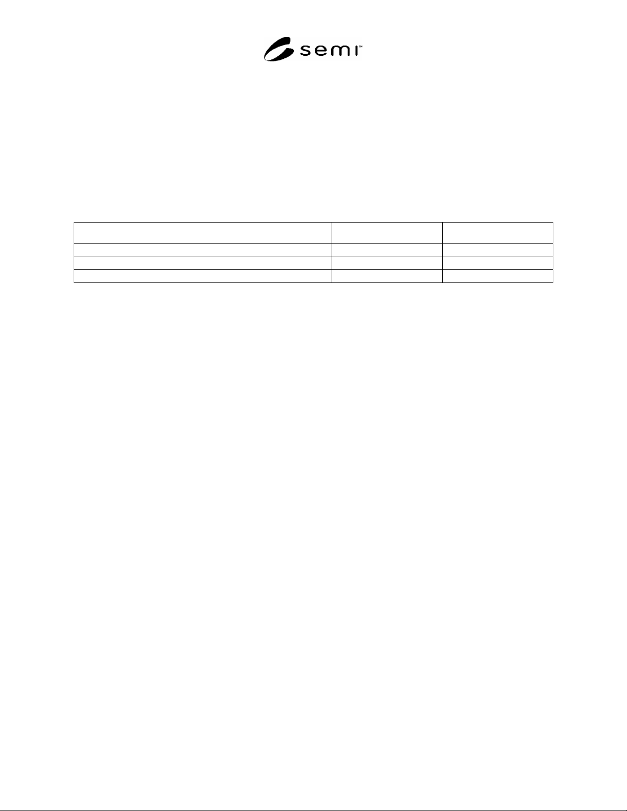
based on the results of the multilaboratory experiment is given in Table 1, which gives the 90th percentile values for
r
and
R
in each category. The 90th percentile value is the value of
r
or
R
below which 90% of the contributed
values for that parameter in that category fall. It is expected to be a conservative estimate of
r
or
R
about 90% of
the time for predicting the precision achievable by a well-controlled laboratory. The use of percentile distributions
of the test data to obtain these estimates of
r
and
R
for the entire resistivity range results in a high value for the
SEMI MF525-0705 © SEMI 2003, 2005 10
reproducibility value of silica-polished specimens which serves as a clear warning of the variability of results
incurred with the silica process.
16.3 These components of random error and their propagation to estimate overall measurement precision are
applicable only to single laboratory-operator-instrument circumstances. No estimate of interlaboratory precision
was derived from this multilaboratory experiment.
NOTE 10: These estimates of random error were based on data from laboratories that gave evidence of being in control of the
specimen preparation and measurement processes. They are values that should be obtainable by any laboratory which is in
control of the measurement process. However, they are superseded by whatever improved values of precision an individual
laboratory can verify it obtains.
Table 1 Estimates of Repeatability,
r
, and Reproducibility,
R
, of Spreading Resistance Measurements as a
Function of Specimen Preparation for Wafers with Resistivity in the Range of 0.01 to 200
·cm
Surface Preparation
r
, %
R
, %
Diamond-planar polished 3.4 6.4
Diamond-bevel polished 6.3 6.2
Silica-bevel polished 4.9 19
16.3.1 These estimates are expected to apply directly to measurements made with probe loads in the range from 10
to 45 g. They are expected to be quite conservative estimates for measurements made at the upper end of this probe
load range, and are expected to be less conservative for measurements made at the lower end of the range. There
were too few data at 5 g in the multi-laboratory test to apply them with confidence to measurements made at this low
a probe load.
16.4 Details of the analysis of the multi-laboratory test are given in Related Information 1. Related Information 2
gives procedures to combine the components of error in order to estimate the total random error, or precision, to be
expected in obtaining spreading resistance data and in converting such data to resistivity values by use of empirical
calibration. These procedures are applied to the results of the multilaboratory experiment to provide an example of
their use. They may also be used with values
r
and
R
derived from in-house experimentation to provide an
estimate of the precision to be expected in a particular location. Related Information 3 lists some sources of
systematic error which may be encountered.
16.5 The bias of this test method cannot be evaluated because there are no available reference standards suitable
for evaluating bias.
17 Keywords
17.1 calibration; epitaxial layer; resistivity; silicon; spreading resistance; spreading resistance probe