semi合集-English.pdf - 第7258页
SEMI MF657-0705 © SEMI 2003, 2005 4 7.1.4 Surface Plate — Granite, with a working surface at least large enough t o accommodate th e largest ring to be used, meeti ng the requirem ents of Laboratory Grade AA a s given in…

SEMI MF657-0705 © SEMI 2003, 2005 3
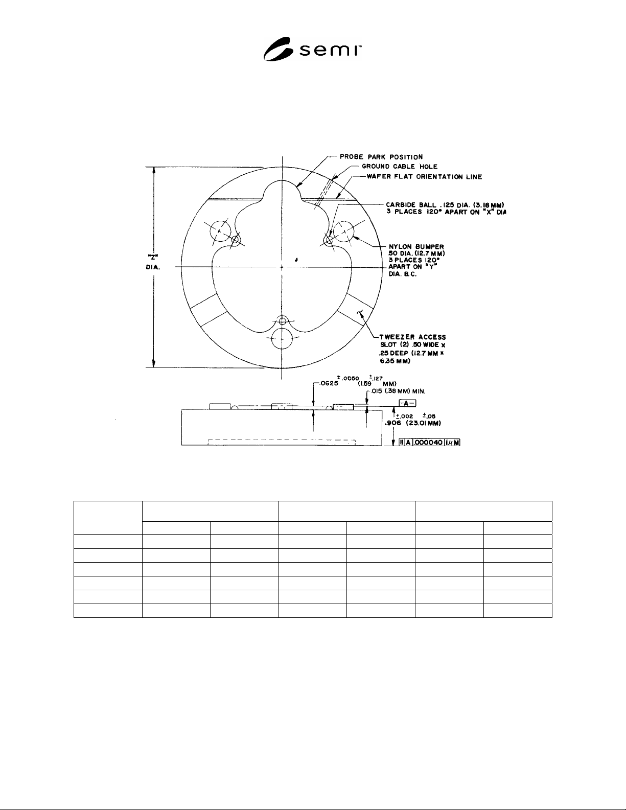
7.1.1 Reference Ring — Consisting of a closed base and three hemispherical support pads (see Figure 1); a different
size ring is required for use with each diameter of wafer to be measured (see Table 1). Each reference ring shall be
fabricated of a metal whose thermal coefficient of expansion shall not exceed 11 10
6
/C (or 6 × 10
6
/°F) at
laboratory temperatures; be at least 19 mm (or 0.75 in.) thick, with the bottom surface lapped flat to within 250 nm
(or 10 in.); have an outside diameter approximately 50 mm (or 2 in.) larger than the nominal diameter of the
specimen wafer with which it is intended to be used; and incorporate the following features:
7.1.1.1 Three Hemispherical Support Pads — Used to define the plane of the reference ring and equally spaced
within ±130 m (or 0.005 in) on the circumference of a circle whose diameter is 6.35 mm (or 0.250 in.) less than
the nominal diameter of the wafer as given in SEMI M1. The support pads shall be fabricated from tungsten
carbide, or from a material of the same or greater hardness, have a nominal diameter of 3.18 mm (or 0.125 in.), and
project 1.59 0.13 mm (or 0.0625 ± 0.0050 in.) above the upper surface of the reference ring. The upper bearing
surface of each support pad shall be polished, with a maximum surface roughness R
A
of 250 nm (or 10 in.)
measured with 0.8 mm (or 0.31-in) cutoff in accordance with ANSI/ASME B 46.1.
7.1.1.2 Three Cylindrical Guide Pins — Used to assist the operator to position the specimen wafer by eye, spaced
approximately equally on the circumference of a circle whose diameter is nominally equal to the sum of the
diameter of the pin and the maximum allowable wafer diameter as given in SEMI M1. The guide pins shall be at
least 380 m (or 0.015 in.) higher than the support pads (see Figure 1).
7.1.1.3 Probe Parking Position — Cut-out area in the reference ring outside the nominal wafer diameter to permit
the ring to be positioned so that the probe assembly is out of the way for specimen or precision flat insertion and
removal (see Figure 1).
NOTE 1: The plane defined by the reference ring is the plane tangent to the three pads.
NOTE 2: It is recommended that the guide pins be fabricated from a hard plastic material.
7.1.2 Probe Assembly with Indicator — Paired, non-contacting, displacement-sensing probes, probe supports, and
indicator unit. The probes shall be capable of independent measurement of the distance between the probed site on
each surface of the specimen slice and the plane of the reference ring. The probes shall be mounted above and
below the specimen position in a manner so that the probe site on one surface of the specimen is opposite the probed
site on the other. The common axis of mounting shall be perpendicular (±2°) to the plane defined by the reference
ring. The upper probe mount shall incorporate a positioning adjustment to accommodate the wafer thickness range
desired. The indicator unit shall be capable of displaying the output from each probe individually and of being
manually reset. The assembly shall satisfy the following requirements:
7.1.2.1 Probe-sensing area (probed site) diameter shall be in the range from 1.55 to 5.75 mm (or 0.062 to 0.225 in),
7.1.2.2 Displacement resolution of 250 nm (or 10 in) or better from a probed site,
7.1.2.3 Displacement range (for each probe) of at least ±0.010 in. (±0.25 mm) about the nominal zero position,
7.1.2.4 Linearity within 0.5% of the full-scale reading, and
7.1.2.5 For instruments operating in an automatic data-sampling mode during scan, sampling capability of at least
100 data points per second.
NOTE 3: The probe-sensing principle may be capacitive, optical, or any other noncontacting means suitable for determinating
the separation between probe and silicon surface; noncontacting is specified to prevent the probe from deflecting the specimen
wafer.
NOTE 4: The indicator unit may conveniently incorporate (1) means for calculating and storing sums or differences of paired
displacement measurements and for identifying the maximum and minimum values of these quantities, (2) means for zero-
reading adjustment, and (3) switch-selectable display of stored calculated values, individual probe measurements, and the like.
The display may be digital or analog (dial); digital readout is recommended to eliminate interpolative errors on the part of the
operator.
7.1.3 Guide — Means for restricting the motion of the reference ring so that the probe mounting axis does not
approach closer to the edge of the specimen wafer than 6.78 mm (or 0.267 in) except at the parking position.
NOTE 5: Depending on the design of the apparatus, a matching guide may be required for each reference ring.
SEMI MF657-0705 © SEMI 2003, 2005 4
7.1.4 Surface Plate — Granite, with a working surface at least large enough to accommodate the largest ring to be
used, meeting the requirements of Laboratory Grade AA as given in Federal Specification GGG-P 463C, and with
provision for accommodating the lower probe mount.
7.2 System Mechanical Parallelism — With the reference ring in position on the surface plate, the distance between
the top of each pad and the upper surface of the plate shall be equal to within 1.0 mm (or 40 in.).
Figure 1
Reference Ring
Table 1 Dimensions of Reference Ring (see Figure 1)
X Y Z
Nominal Wafer
Diameter
in. mm in. mm in. mm
2 in. 1.750 44.45 2.515 63.88
4.00 101.6
3 in. 2.750 69.85 3.525 89.54
5.00 127.0
100 mm 93.65 113.20
150.0
125 mm 118.65 138.20
175.0
150 mm 143.65 163.20
200.0
200 mm 193.65 213.20
300.0
SEMI MF657-0705 © SEMI 2003, 2005 5
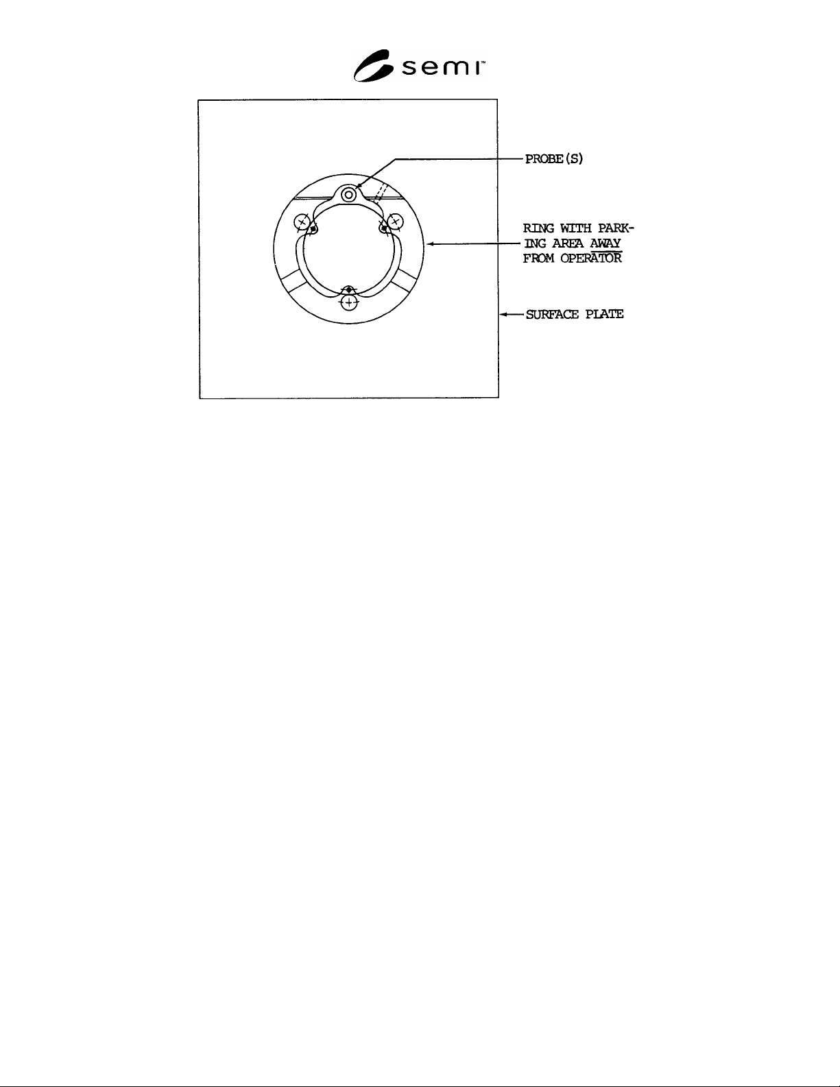
Figure 2
Orientation of Reference Ring
7.3 Set-up Thickness Masters — Covering a range equal to the nominal thickness of the wafer to be tested ±125 m
(or 0.005 in.), in approximately 50 m (or 0.002 in.) steps (a total of 6 masters). Each master shall have surfaces
flat to within 250 nm (or 10 in.) and a thickness variation no greater than 1.25 m (or 50 in.). The thickness of
each master shall be known to within 1.25 m (or 50 in.). The diameter of each master shall be suitable for the
ring with which it will be used.
NOTE 6: Silicon wafers satisfying the above requirements may be used as set-up thickness masters.
7.4 Precision Metal Flat — Of the same nominal diameter as the wafer to be tested and with one surface flat to 0.2
m (or 8 in.) TIR, maximum. The thickness of the flat shall be such as to permit the flat to be placed and
measured in the specimen position (see ¶9.2).
8 Sampling
8.1 This test method is nondestructive and may be used on either a 100% or a sampling basis.
8.2 If samples are to be taken, procedures for selecting the sample from each lot of wafers to be tested shall be
agreed upon by the parties to the text, as shall the definition of what constitutes a lot.
9 Calibration and Standardization
9.1 Through measurements on set-up thickness masters sized according to the nominal diameter of the intended
specimen wafer (see ¶7.3), calibrate and qualify the apparatus as follows:
9.1.1 If not already assembled, assemble the apparatus with the selected reference ring, corresponding to the
intended specimen size, on the surface plate and the guide in position to limit ring movement. Make sure that the
probes are in the parking position and that the position is away from the operator (see Figure 2).
9.1.2 Make, record, and analyze measurements on each selected setup thickness master in turn, in accordance with
the manufacturer's instructions or in accordance with the sections on procedure and calculations (§10 and Figure 4).
Position the ring so that the probes are in the parking position before inserting or removing a master.
9.1.3 Construct a plot of measured thickness of each master as a function of known thickness. Draw a straight line
through the end points. At each end point, plot two additional points representing values of +0.5% and 0.5% of the
end point values. Draw a limit line through the two +0.5% values. Draw another limit line through the two 0.5%