semi合集-English.pdf - 第7274页
SEMI MF674-0705 © SEMI 2003, 2005 5 finish with the microscope . Compare the finish with the appr opriate photo g raph of Fi gure 2, which shows results obtainable wi th differe n t size diam ond in the range specified f…

SEMI MF674-0705 © SEMI 2003, 2005 4
10.2 Sample Mounting Block and Fixture — For holding the silicon specimen at the desired beveling angle during
the bevel-polishing process.
10.3 Microscope — Optical microscope having a total magnification of at least 30× and a system for illuminating
the stage obliquely.
10.4 Hot Plate, capable of heating the mounting block and wax to 150°C.
11 Reagents and Materials
11.1 Diamond Slurry — Synthetic or natural diamond with a grain size in the range 0.05 to 0.25 m, inclusive,
suspended in a liquid or paste carrier.
11.2 Solvent — Suitable nonaqueous solvent for removing diamond slurry subsequent to polishing (see Note 5).
11.3 Wax — Glycol phthalate or other similar wax having a melting temperature of less than 150°C.
11.4 Wipe, Lint-Free Paper, or Cloth — Suitable for cleaning the glass plate.
11.5 Oil Extender — Compatible with the diamond slurry (see ¶11.1).
12 Procedure
12.1 Prior to beveling each specimen, clean the frosted surface of the glass plate by swabbing with the solvent using
the lint-free wipe.
NOTE 9: Because of the rigidity of the glass surface, excessive damage to the beveled silicon surface can result from
contamination of the polishing slurry with foreign material whose size is larger than that of the diamond grit.
12.2 Apply a small amount of diamond slurry (or paste) to the surface of the glass. Distribute the slurry (or paste)
with a clean flexible metal or plastic spatula or other lint-free applicator so that a thin, uniform film results over an
area whose dimensions are several times larger than the lateral dimension of the fixture used to support the beveling
block. An oil extender may be used to prolong the life of the slurry. The oil extender generally slows the cutting
somewhat and aids lubrication during beveling.
12.3 With the hot plate, heat the mounting block to the melting temperature of the wax. Mount the silicon specimen
to the block with the wax. Allow the block to cool to room temperature.
12.4 Assemble the sample mounting block with specimen attached to the mounting fixture, and place this assembly
on the glass plate. Lower the piston of the polishing fixture carefully and gently onto the glass plate to minimize the
risk of chipping or otherwise damaging the silicon chip.
12.5 Polish the specimen by orbital, figure-eight, or reciprocating movement of the polishing fixture over the glass
plate.
NOTE 10: Use of the above polishing procedure, wherein the specimen and its fixture are moved upon a stationary glass plate,
risks the generation of random deep scratches on the beveled surface due to accumulated coarse debris on the polishing plate. It
has been found that using a rotating glass plate while holding the specimen mounting fixture so that the leading edge of the
beveled chip always faces into the direction of plate rotation reduces the risk. However, if each chip to be beveled is positioned
at the same, or nearly the same, radial distance from the plate's center of rotation, uneven wear of the plate in the form of a
channel, or wide groove, is likely to result. Such channeling of the polishing plate can be minimized or eliminated either by
moving the specimen mounting fixture slowly along the plate radius while polishing, or by choosing a different radial position on
the plate for each chip to be beveled.
12.6 Clean and inspect the specimen periodically to determine whether an adequate amount of specimen surface has
been exposed by beveling (see Note 5).
12.7 Repeat ¶12.5 and ¶12.6 as necessary until an adequate extent of beveled surface is obtained.
NOTE 11: At the beginning of the beveling process an extremely small area of silicon supports the static load of the polishing
assembly, and pressures on the silicon are extremely high. To minimize the possibility of fracture of the edge of the silicon chip,
it has been found advisable to begin bevel polishing with a relatively slow rate of motion of the polishing assembly.
12.8 When the desired amount of specimen surface has been exposed by beveling, thoroughly clean the specimen
by flushing or swabbing with the appropriate organic solvent (see ¶11.2). Inspect the beveled surface for quality of
SEMI MF674-0705 © SEMI 2003, 2005 5
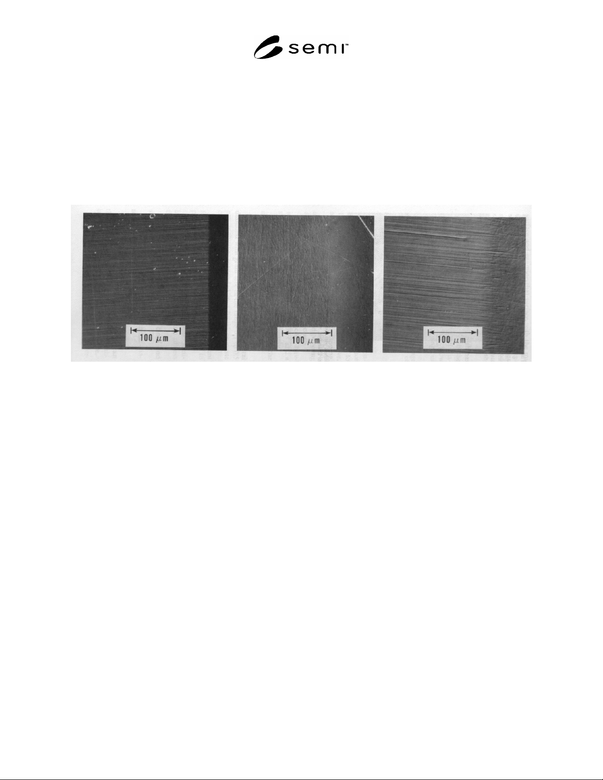
finish with the microscope. Compare the finish with the appropriate photograph of Figure 2, which shows results
obtainable with different size diamond in the range specified for two types of motion during polishing. Repolish
lightly if the finish appears to be significantly coarser than that shown in the appropriate photograph. Use dry air or
nitrogen to blow the specimen surface dry prior to carrying out any spreading resistance measurements.
NOTE 12: Clean the polishing plate regularly to remove coarse polishing residue or air-borne contaminants. This cleaning can
be done with a lint–free cloth or paper wipe and the same solvent used to clean polishing residue from the specimen. Inspect the
plate when clean. If it shows signs of scratching, burnish marks, or areas where the lapped finish has been polished smooth, relap
the plate then clean thoroughly to remove lapping debris and broken-in on scrap samples (see Note 13).
NOTE 13: A newly-frosted glass plate may not yield optimum results. Such a plate can be improved by preparing a number of
samples of scrap silicon before beveling the test specimen of interest. The best indicator of frosted glass plate condition is the
quality and uniformity of surface damage on the finished bevel.
a. 0.1
m Diamond, b. 0.1 m Diamond, c. 0.5 m Diamond,
Reciprocating Motion Figure-of-Eight Motion Reciprocating Motion
Figure 2
Surface Texture of Silicon Specimens Bevel-Sectioned with Diamond Against Ground-Glass Surface
13 Keywords
13.1 beveling; diamond polishing; resistivity; resistivity variations; sample preparation; semiconductor; silicon;
spreading resistance; spreading resistance probe (SRP)
NOTICE: SEMI makes no warranties or representations as to the suitability of the standards set forth herein for any
particular application. The determination of the suitability of the standard is solely the responsibility of the user.
Users are cautioned to refer to manufacturer's instructions, product labels, product data sheets, and other relevant
literature, respecting any materials or equipment mentioned herein. These standards are subject to change without
notice.
By publication of this standard, Semiconductor Equipment and Materials International (SEMI) takes no position
respecting the validity of any patent rights or copyrights asserted in connection with any items mentioned in this
standard. Users of this standard are expressly advised that determination of any such patent rights or copyrights, and
the risk of infringement of such rights are entirely their own responsibility.
Copyright by SEMI® (Semiconductor Equipment and Materials
International), 3081 Zanker Road, San Jose, CA 95134. Reproduction of
the contents in whole or in part is forbidden without express written
consent of SEMI.

SEMI MF928-0305 © SEMI 2005 1
SEMI MF928-0305
TEST METHODS FOR EDGE CONTOUR OF CIRCULAR
SEMICONDUCTOR WAFERS AND RIGID DISK SUBSTRATES
These test methods were technically approved by the Global Silicon Wafer Committee and are the direct
responsibility of the North American Silicon Wafer Committee. Current edition approved for publication by
the North American Regional Standards Committee on December 10, 2004 Initially available at
www.semi.org January 2005; to be published March 2005. Original edition published by ASTM
International as ASTM F 928-85. Last previous edition SEMI MF928-02.
1 Purpose
1.1 The edges of circular wafers of electronic materials are frequently required to be shaped after cutting the wafers
from the ingot. Contouring the wafer edge reduces the incidence of chipping and minimizes epitaxial edge crown
and photoresist edge bead during subsequent processing of the wafer. Similarly, edges of rigid disk substrates are
frequently edge shaped.
1.2 The test methods described here provide means to determine that the wafer edge contour is appropriate to meet
specifications, such as SEMI M1 or SEMI M9, which are intended to provide wafers avoiding the difficulties
enumerated above.
2 Scope
2.1 These test methods provide means for examining the edge contour of circular wafers of silicon, gallium
arsenide, and other electronic materials, and determining fit to limits of contour specified by a template that defines
a permitted zone through which the contour must pass. Principal application of such a template is intended for, but
not limited to, wafers that have been deliberately edge shaped.
NOTE 1: DIN 50441/2 is equivalent to Method B of this standard. It is the responsibility of DIN Committee NMP 221. DIN
50441/2, Measurement of the Geometric Dimensions of Semiconductor Slices; Testing of Edge Rounding, is available from
Beuth Verlag GmbH, Burggrafenstrasse 6, 10787 Berlin, Germany, Telephone: 49.30.2601-0, Fax: 49.30.2601.1263, Website:
www.beuth.de.
2.2 Two test methods are described.
2.2.1 Method A is destructive and is limited to inspection of discrete points on the periphery, including flats. The
contour of deliberately edge-shaped wafers may not be uniform around the entire periphery, and thus the discrete
location(s) may or may not be representative of the entire periphery.
2.2.2 Method A is recommended for examining the edge profile of flatted regions of the wafer.
2.2.3 Method A is best suited for referee purposes.
2.3 Method B is nondestructive and suitable for inspection of all points on the wafer periphery except flats.
2.3.1 Method B is appropriate for routine process monitoring such as alignment of wafer edge grinders, routine
quality control and incoming/outgoing inspection purposes. In view of the uncertainty of precisely locating the
intersection of the contour and the wafer surface when carrying out Method B, use of this method for commercial
transactions is not recommended unless the parties to the test establish the degree of correlation that can be obtained.
2.3.2 Method B may also be applied to the examination of the edge contour of the outer periphery of substrates for
rigid disks used for magnetic storage of data; metallic rigid disk substrates cannot conveniently be cleaved.
NOTE 2: Reference to wafers in the remainder of this standard shall be interpreted to include substrates for rigid disks unless the
phrase “of electronic materials” is also included in the context.
2.4 The values stated in SI units are to be regarded as the standard. The values given in parentheses are for
information only.
NOTICE: This standard does not purport to address safety issues, if any, associated with its use. It is the
responsibility of the user of this standard to establish appropriate safety and health guides and determine the
applicability of regulatory or other limitations prior to use.