semi合集-English.pdf - 第7284页
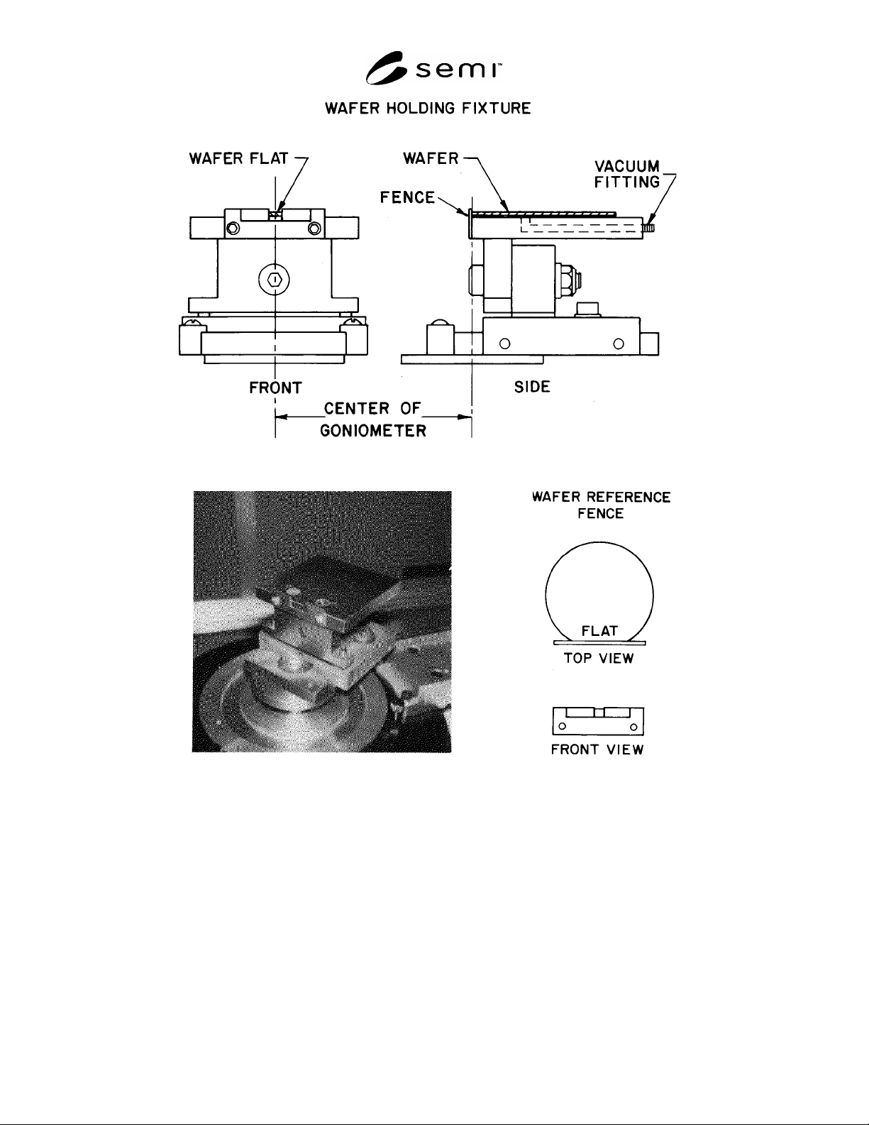
SEMI MF847-0705 © SEMI 2003, 2005 4 a. Front and Side Views b. Photograph of Mounte d Fixture c. Detail of Wafer and Reference Fence Figure 1 Wafer Holdin g Fixture for X -Ray E dge Diffr action Method 9.2.1 The horizont…

SEMI MF847-0705 © SEMI 2003, 2005 3
6 Hazards
6.1 These test methods use X radiation; it is absolutely necessary to avoid personal exposure to X rays.
6.1.1 It is especially important to keep hands or fingers out of the path of the X rays and to protect the eyes from
scattered secondary radiation.
6.1.2 The use of commercial film badge or dosimeter service is recommended, together with periodic checks of the
radiation level at the hand and body positions with a Geiger-Muller counter calibrated with a standard nuclear
source.
NOTE 2: The present maximum permissible dose for total body exposure of an individual to external X-radiation of quantum
energy less than 3 MeV over an indefinite period is 1.25 R (3.22 × 10
4
C/kg) per calendar quarter (equivalent to 0.6 mR/h
(1.5 × 10
7
C/kg·h)) as established in the Code of Federal Regulations, Title 10, Part 20. The present maximum permissible dose
of hand and forearm exposure under the same conditions is 18.75 R (4.85 × 10
3
C/kg) per calendar quarter (equivalent to 9.3
mR/h (2.4 × 10
6
C/kg·h)). Besides the above stated regulations, various other government and regulatory organizations have
their own safety requirements.
6.1.3 It is the responsibility of the user to make sure that the equipment and the conditions under which it is used
meet applicable regulations.
7 Sampling
7.1 Unless otherwise specified, ASTM Practice E 122 shall be used.
7.2 When so specified, appropriate sample sizes shall be selected from each lot according to ANSI/ASQC Z1.4.
7.3 Inspection levels shall be agreed upon between the parties to the test.
TEST METHOD A — X-RAY EDGE DIFFRACTION METHOD
8 Summary of Test Method
8.1 In this test method a holding fixture that uniquely orients the wafer being tested with respect to its geometric
features is used to position the wafers with respect to the X-ray goniometer.
8.2 The goniometer is rotated to determine the Bragg angle with respect to the geometric features by X-ray
diffraction from the crystallographic planes of the wafer edge, first with the wafer front surface up and then with
front surface down.
8.3 The average angular deviation is calculated from the goniometer readings.
9 Apparatus
9.1 X-ray and Goniometer Apparatus — In accordance with ¶5.1 of SEMI MF26, except that the X-ray beam shall
be collimated using a vertical slit.
9.2 Wafer-Holding Fixture, to orient the sample wafer uniquely with respect to the X-ray goniometer (see Figure 1).
The fixture must include a vacuum hold-down with a flat horizontal surface and a reference fence perpendicular to
this surface. These components establish an x-y axis that is fixed with respect to the goniometer and the X-ray
beam. The exact dimensions of the fixture depend on the layout of the X-ray apparatus. The critical features are:
SEMI MF847-0705 © SEMI 2003, 2005 4
a. Front and Side Views
b. Photograph of Mounted Fixture c. Detail of Wafer and Reference Fence
Figure 1
Wafer Holding Fixture for X-Ray Edge Diffraction Method
9.2.1 The horizontal surface must be parallel to the plane of the X-ray beam so that the diffracted beam impinges on
the detector (see Figure 2).
9.2.2 Both the side of the reference fence against which the wafer flat is located, and the fixture surface to which
the reference fence mates, must be flat to within one part in 10,000.
SEMI MF847-0705 © SEMI 2003, 2005 5
10 Procedure
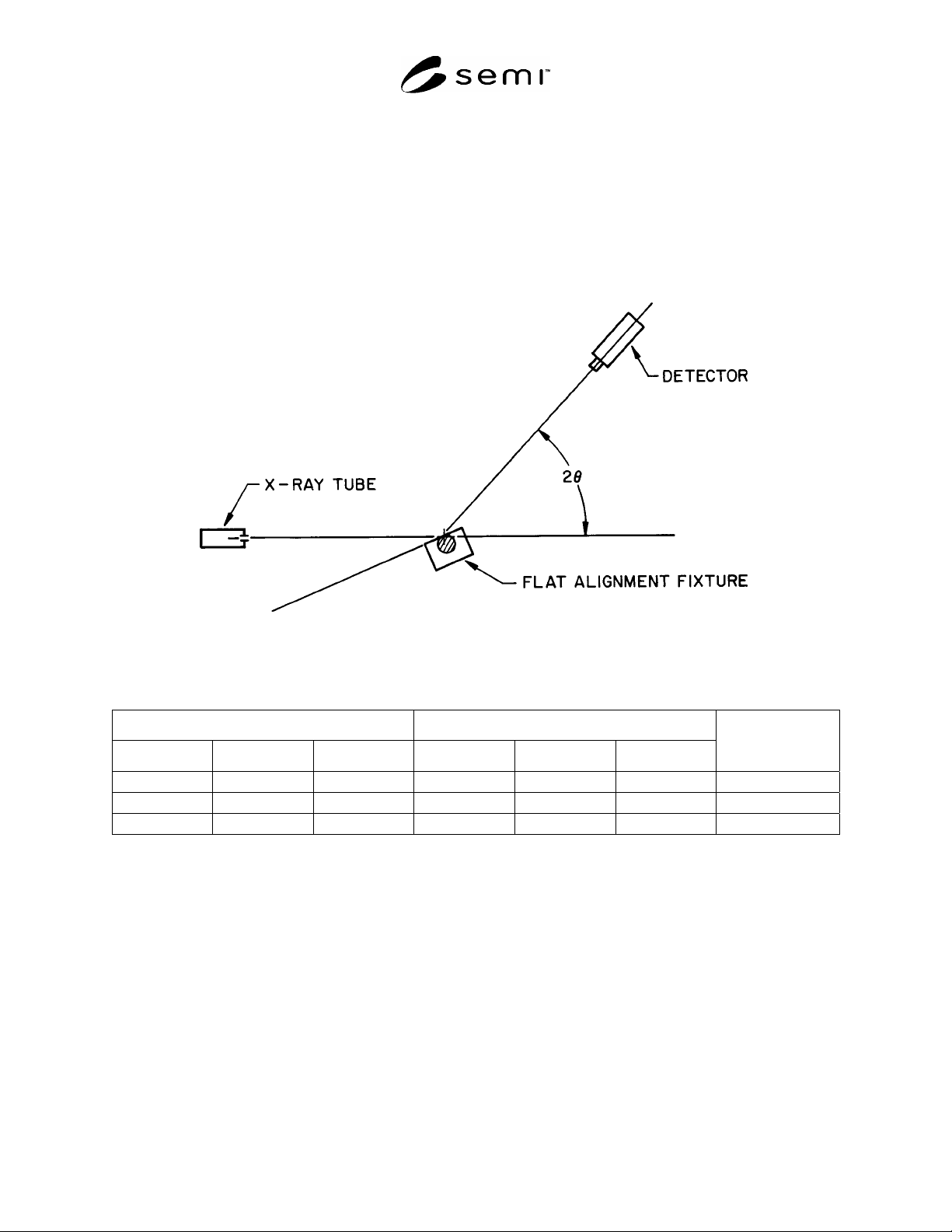
10.1 Position the detector so that the angle between the extension of the incident X-ray beam and the line joining
the detector and the axis of rotation of the specimen is equal (to the nearest minute) to twice the Bragg angle
(see Figure 2).
NOTE 3: This angle (twice the Bragg angle) is listed in Table 1 for CuK radiation for the recommended reflecting planes
corresponding to common silicon wafer flat locations.
10.2 Place the wafer to be tested on the fixture, front surface up. Take care to ensure that the flat is securely located
against the reference fence and activate the vacuum holddown.
Figure 2
Schematic of the Diffraction Geometry for the X-Ray Edge Diffraction Method
Table 1 Bragg Angles,
, for X-Ray Diffraction of Cu-K Radiation in Silicon Crystal
#1
Flat Location Recommended Reflecting Plane
h
k l h k l
Detector Location (2
times Bragg Angle)
1 1 0 2 2 0
4720
2 1 1 4 2 2
8808
1 0 0 4 0 0
6912
#1
Wavelength
= 1.5417 Å.
10.3 With the goniometer movement mechanism, adjust the fixture about the axis of rotation perpendicular to the
incident and reflected beams until the diffracted intensity is at a maximum.
10.4 Record to the nearest 1 min, as
1
, the angle that is indicated on the goniometer.
10.5 Remove the wafer from the fixture, turn it over so that the front surface is now down. Again, take care to
ensure that the flat is securely located against the reference fence and activate the vacuum holddown.
10.6 With the goniometer movement mechanism, adjust the fixture about the axis of rotation perpendicular to the
incident and reflected beams until the diffracted intensity is at a maximum.
10.7 Record to the nearest 1 min, as
3
, the angle that is indicated on the goniometer.