semi合集-English.pdf - 第7289页
SEMI MF847-0705 © SEMI 2003, 2005 9 16.3.1 Align the scri bed line on the un derside of the drafting hea d protractor with the two li ght-generated dots that define the hori zontal reference line and set the protracto r …
SEMI MF847-0705 © SEMI 2003, 2005 8
15.2.4 Camera Mounting Fixture — For clamping the camera to the mounting track so that the collimator is aligned
with the X-ray beam and the horizontal reference line established by the light-generated dots is parallel with the
upper surface of the mounting track to 1 min of arc (29 m in 100 mm).
15.3 Drafting Head Protractor — With a clear plastic blade and finest vernier divisions of six min of arc or less for
reading the Laue photograph. A straight line, approximately 125 mm (or 5 in.) long, and in line with the centerpoint
of the protractor, is inscribed on the bottom of the plastic blade.
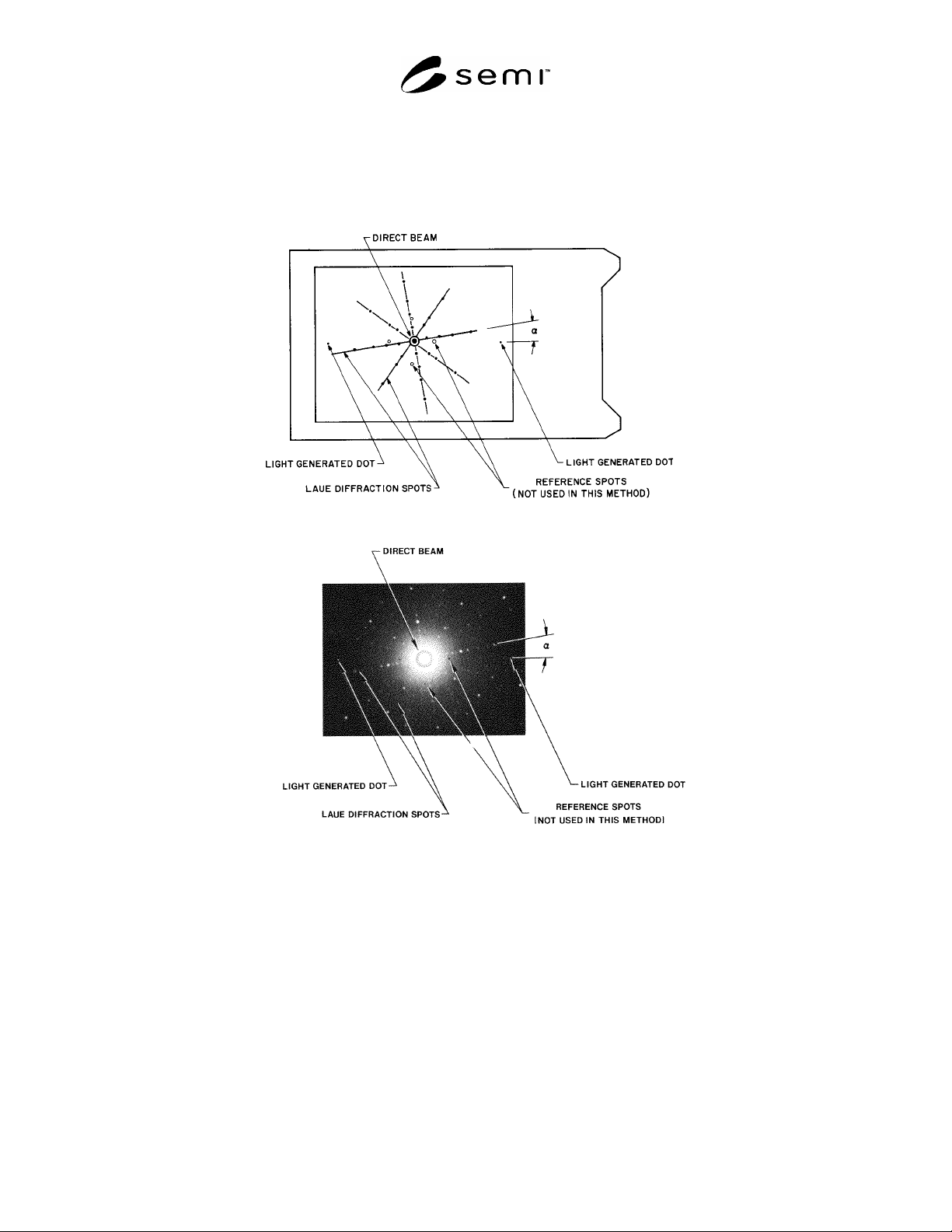
a. Schematic Representation
b. Actual Photograph
Figure 6
Laue Pattern
16 Procedure
16.1 Place the wafer to be tested on the wafer holding fixture so that the flat is resting securely against the reference
flat on the fixture. Turn on the vacuum to hold the wafer securely against the fixture.
16.2 Turn on the X-ray source, adjust the voltage and current (Note 4), and load the film into the camera. Open the
X-ray shutter and expose the film for an appropriate time (Note 5). During exposure, pulse the light to generate the
dots which define the horizontal reference line, and develop the film.
NOTE 4: For a tungsten X-ray tube typical voltage and current are 50 to 60 kV and 20 to 30 mA, respectively.
NOTE 5: Use of high-speed, instant film (ASA 300) and a fluorescent screen results in typical exposure times of 1 to 2 min.
16.3 Read the Laue pattern on the film.

SEMI MF847-0705 © SEMI 2003, 2005 9
16.3.1 Align the scribed line on the underside of the drafting head protractor with the two light-generated dots that
define the horizontal reference line and set the protractor to 0°.
16.3.2 Rotate the protractor so that the scribed line is aligned with the zone of Laue spots that (1) passes through the
center of the pattern and (2) is nearest to the horizontal reference line (see Figure 6).
16.3.3 Read to the nearest 0.1° (6 min) the angle on the protractor and record the value as the angular deviation,
.
17 Report
17.1 Report the following information:
17.1.1 Identity of samples tested including vendor and vendor lot identity,
17.1.2 Date of test and identity of operator making the measurements,
17.1.3 Specified flat and surface orientations,
17.1.4 The measured angular deviation for each wafer, and
17.1.5 The photograph or a copy of the photograph of the Laue pattern for each wafer.
18 Precision and Bias
18.1 The single-instrument, multi-operator precision of this test method was estimated by extensive testing with
three operators. This test yielded a distribution of readings with a 1-s value of 7 min of arc.
19 Keywords
19.1 crystallographic orientation; flats; Laue diffraction; silicon; single crystal
NOTICE: SEMI makes no warranties or representations as to the suitability of the standards set forth herein for any
particular application. The determination of the suitability of the standard is solely the responsibility of the user.
Users are cautioned to refer to manufacturer's instructions, product labels, product data sheets, and other relevant
literature, respecting any materials or equipment mentioned herein. These standards are subject to change without
notice.
By publication of this standard, Semiconductor Equipment and Materials International (SEMI) takes no position
respecting the validity of any patent rights or copyrights asserted in connection with any items mentioned in this
standard. Users of this standard are expressly advised that determination of any such patent rights or copyrights, and
the risk of infringement of such rights are entirely their own responsibility.
Copyright by SEMI® (Semiconductor Equipment and Materials
International), 3081 Zanker Road, San Jose, CA 95134. Reproduction of
the contents in whole or in part is forbidden without express written
consent of SEMI.

SEMI MF951-0305 © SEMI 2003, 2005 1
SEMI MF951-0305
TEST METHOD FOR DETERMINATION OF RADIAL INTERSTITIAL
OXYGEN VARIATION IN SILICON WAFERS
These test methods were technically approved by the Global Silicon Wafer Committee and are the direct
responsibility of the North American Silicon Wafer Committee. Current edition approved for publication by
the North American Regional Standards Committee on December 10, 2004. Initially available at
www.semi.org January 2005; to be published March 2005. Original edition published by ASTM
International as ASTM F 951-85. Last previous edition SEMI MF951-02.
1 Purpose
1.1 The presence of oxygen can be beneficial to certain manufacturing operations by preventing the formation of
process-induced defects. To the extent that this is true, it becomes important that the oxygen be uniformly
distributed over the entire slice.
1.2 Multiple test plans are included to satisfy a variety of requirements. The characteristic shape and magnitude of
oxygen concentration distributions in crystals are functions of the crystal growth process. Although the specified
test plans are intended to cover oxygen concentration distributions which are typically found, other distributions
may occur. In such cases, it may be necessary to use test positions other than those specified in order to adequately
describe the distribution pattern.
1.3 This test method may be used for process control, research and development, and materials acceptance
purposes. In the absence of an interlaboratory evaluation of the precision of this test method, its use for materials
acceptance is not recommended unless the parties involved establish the degree of correlation which can be expected
(see §12).
2 Scope
2.1 This test method covers test site selection and data reduction procedures for radial variation of the interstitial
oxygen concentration in silicon slices typically used in the manufacture of microelectronic semiconductor devices.
2.2 This test method is intended as both a referee and production test through selection of an appropriate test
position plan.
2.3 The interstitial oxygen content may be measured in accordance with SEMI MF1188, SEMI MF1619, DIN
50438/1, JEITA EM-3504, or any other procedure agreed upon by the parties to the test.
NOTE 1: SEMI MF1366 is not based on infrared absorption measurement and it measures total oxygen content, not interstitial
oxygen content. It is also a destructive technique. However, it can be used to determine the radial variation of the oxygen
content if suitable modifications of the test procedure are made.
2.4 Acceptable thickness and surface finish for the test specimens are specified in the applicable test methods. This
test method is suitable for use on chemically etched, single-side polished and double-side polished silicon wafers or
slices with no surface defects that could adversely change infrared radiation transmission through the test specimen
(subsequently called slice), provided that appropriate test methods for oxygen content are selected.
NOTICE: This standard does not purport to address safety issues, if any, associated with its use. It is the
responsibility of the user of this standard to establish appropriate safety and health guides and determine the
applicability of regulatory or other limitations prior to use.
3 Limitations
3.1 Variations of optical thickness can be caused by thickness or surface finish variations, or both.
3.2 Beam size differences from instrument to instrument can cause errors when the beam area is smaller than the
aperture used in this test method.