semi合集-English.pdf - 第7305页
SEMI MF1152-0305 © SEMI 2003, 2005 4 10.5 Align t h e fixt ure using only table cr ossfeed (h orizontal) control and fixture rotation so t hat the simulated pin outline on the template makes contact with the sides of the…
SEMI MF1152-0305 © SEMI 2003, 2005 3
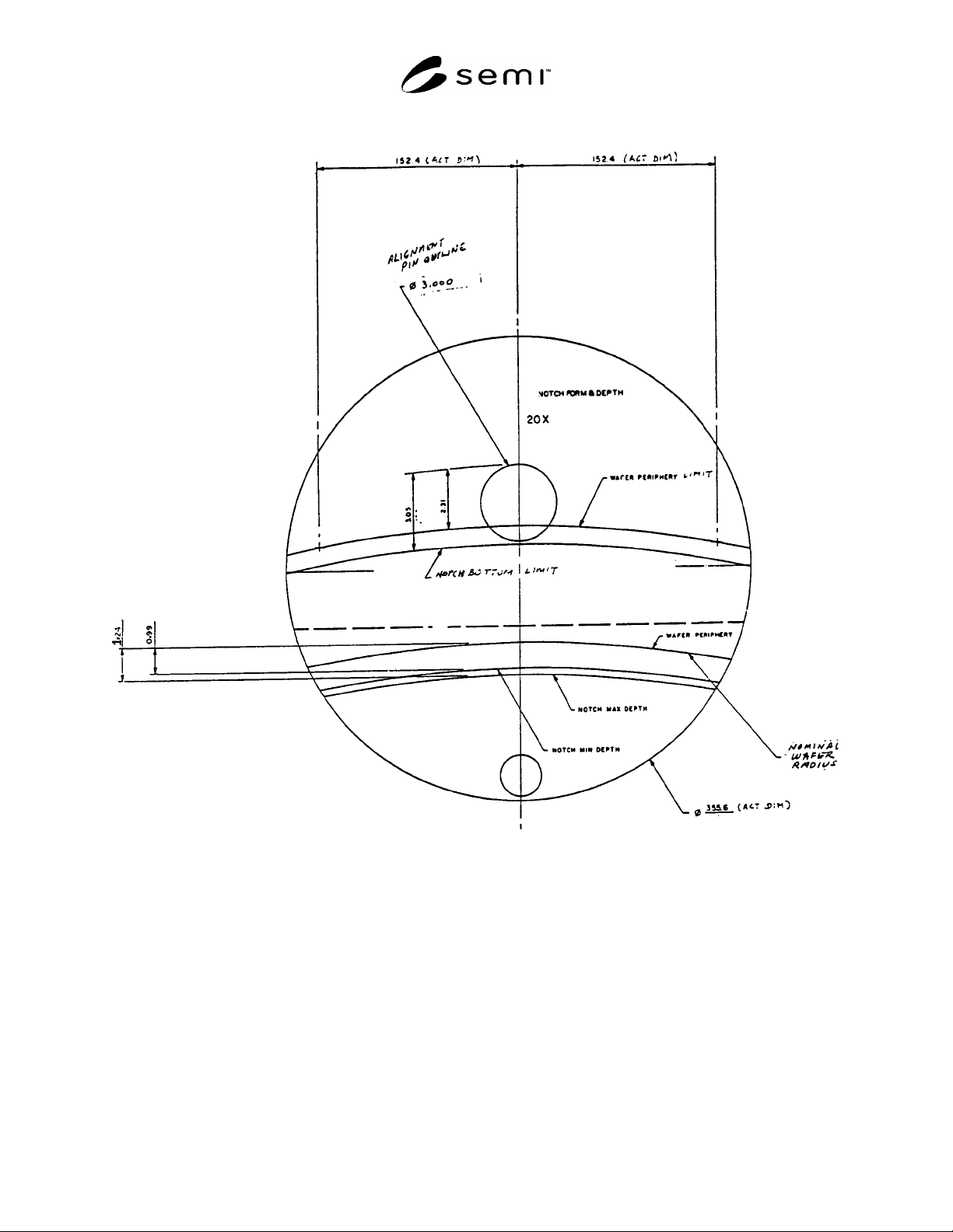
9.3 Include horizontal and vertical axes and label the lines on the notch form and depth template as shown in Figure
1.
NOTE: In use the template is rotated 90° counterclockwise.
Figure 1
Example of Notch Form and Depth Template
10 Procedure
10.1 Set the magnification to 20×.
10.2 Align the fixture in the comparator so that the notch is at the nine o’clock position and the directions of
horizontal and vertical motion of the fixture in the comparator are parallel with and perpendicular to, respectively,
the diameter that passes through the notch.
10.3 Place the notch form and depth template on the comparator screen. Align the horizontal and vertical lines with
the simulated pin outline in the nine o'clock position.
10.4 Place the first wafer to be tested in the fixture, front surface up.

SEMI MF1152-0305 © SEMI 2003, 2005 4
10.5 Align the fixture using only table crossfeed (horizontal) control and fixture rotation so that the simulated pin
outline on the template makes contact with the sides of the notch image.
10.6 Verify that the image of the notch bottom falls on or below the NOTCH BOTTOM LIMIT line. If the image
of the notch bottom falls above this line, record the wafer as defective.
10.7 Verify that the image of the wafer edge falls on or above the WAFER PERIPHERY LIMIT line. If the image
of the wafer edge falls above this line, record the wafer as defective.
10.8 Move the fixture to the right until the image of the wafer edge falls on the line marked WAFER PERIPHERY
using only the table crossfeed control.
10.9 Verify that the notch bottom falls between the NOTCH MAX DEPTH and NOTCH MIN DEPTH lines. If the
image of the notch bottom falls outside these lines, record the wafer as defective.
10.10 Repeat ¶¶10.4 through 10.9 for all remaining wafers to be tested.
10.11 Remove the notch form and depth template and replace it with the notch angle template.
10.12 Set the magnification to 50×.
10.13 Place the first wafer to be tested in the fixture, front surface up.
10.14 Align the image of the wafer notch sides with each angle on the template using the table crossfeed control
and the fixture rotation. Define as the notch angle, the angle that provides the best fit to the image. If the notch
angle is < 89 or > 95°, record the wafer as defective.
10.15 Repeat ¶10.14 for all remaining wafers to be tested.
10.16 On completion of the testing, return the magnification to 20×.
11 Report
11.1 Report as a minimum the following information:
11.1.1 Date of test,
11.1.2 Name of person conducting the test,
11.1.3 The lot number of other identification of the material,
11.1.4 The number of wafers in the lot,
11.1.5 The number of test wafers, and
11.1.6 The number of defective wafers.
11.2 If desired, a table of the types of defects observed may be provided.
12 Precision and Bias
12.1 An interlaboratory evaluation of this test method has not been executed, nor is one anticipated. Use of the test
method for commercial transactions is not recommended unless the parties to the test establish the degree of
correlation that can be obtained.
12.2 A dimension of 0.1 mm in the object plane produces a screen image of 2.0 mm at 20× and of 5.0 mm at 50×.
The smallest size details of the notch contour which can be inspected by this test method are of comparable
dimensions.
13 Keywords
notch; notch dimension; optical comparator; silicon; wafer

SEMI MF1152-0305 © SEMI 2003, 2005 5
NOTICE: SEMI makes no warranties or representations as to the suitability of the standards set forth herein for any
particular application. The determination of the suitability of the standard is solely the responsibility of the user.
Users are cautioned to refer to manufacturer's instructions, product labels, product data sheets, and other relevant
literature, respecting any materials or equipment mentioned herein. These standards are subject to change without
notice.
By publication of this standard, Semiconductor Equipment and Materials International (SEMI) takes no position
respecting the validity of any patent rights or copyrights asserted in connection with any items mentioned in this
standard. Users of this standard are expressly advised that determination of any such patent rights or copyrights, and
the risk of infringement of such rights are entirely their own responsibility.
Copyright by SEMI® (Semiconductor Equipment and Materials
International), 3081 Zanker Road, San Jose, CA 95134. Reproduction of
the contents in whole or in part is forbidden without express written
consent of SEMI.