semi合集-English.pdf - 第736页
SEMI E99.1-1104 © SEMI 2000, 2004 5 RELATED INFORMATION 1 SCENARIOS NOTICE : This related information is not an official part of SEMI E99.1. This related information was approved for publication by full letter ballot pro…

SEMI E99.1-1104 © SEMI 2000, 2004 4
NOTICE: SEMI makes no warranties or representations as to the suitability of the standard set forth herein for any
particular application. The determination of the suitability of the standard is solely the responsibility of the user.
Users are cautioned to refer to manufacturer’s instructions, product labels, product data sheets, and other relevant
literature respecting any materials mentioned herein. These standards are subject to change without notice.
The user’s attention is called to the possibility that compliance with this standard may require use of copyrighted
material or of an invention covered by patent rights. By publication of this standard, SEMI takes no position
respecting the validity of any patent rights or copyrights asserted in connection with any item mentioned in this
standard. Users of this standard are expressly advised that determination of any such patent rights or copyrights, and
the risk of infringement of such rights, are entirely their own responsibility.
SEMI E99.1-1104 © SEMI 2000, 2004 5
RELATED INFORMATION 1
SCENARIOS
NOTICE: This related information is not an official part of SEMI E99.1. This related information was approved for
publication by full letter ballot procedures on January 14, 2000.
This section provides examples of typical scenarios for a Carrier ID Reader/Writer.
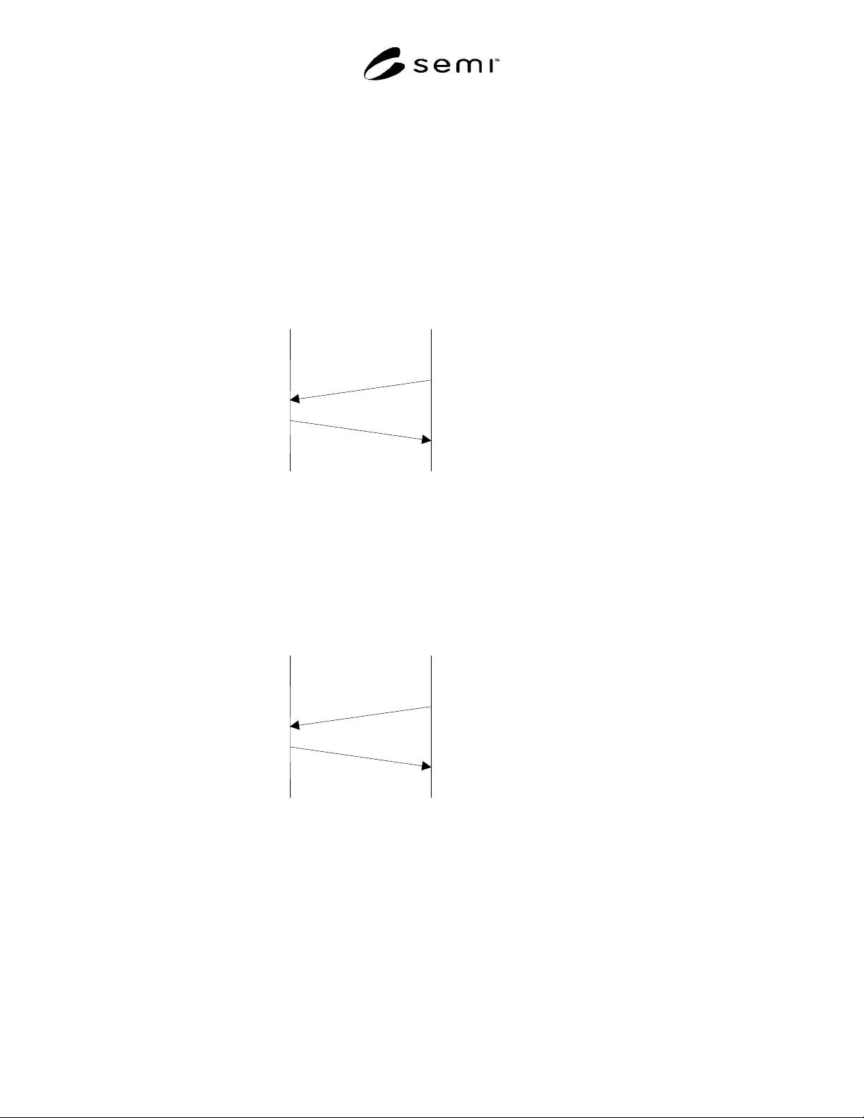
R1-1 Read ID
R1-1.1 The upstream controller sends a Read ID Request message to the CIDRW for Head 1. The CIDRW Head 1
reads the ID, and the CIDRW returns the ID to the upstream controller.
CIDRW
Upstream
Controller
S18,F9 Read ID Request
Target ID = “01”
S18,F10 Read ID Data
MID = “XYZ001”
Figure R1-1
Read ID Scenario
R1-2 Read Data
R1-2.1 The upstream controller sends a Read Data Request message to the CIDRW for Head 1 and DataSeg 1. The
CIDRW Head 1 reads the data, and the CIDRW returns the data to the upstream controller.
CIDRW
Upstream
Controller
S18,F5 Read Request
Target ID = “01”
DataSeg = “0”
S18,F6 Read Data
Data = “yyyyy”
Figure R1-2
Read Data Scenario
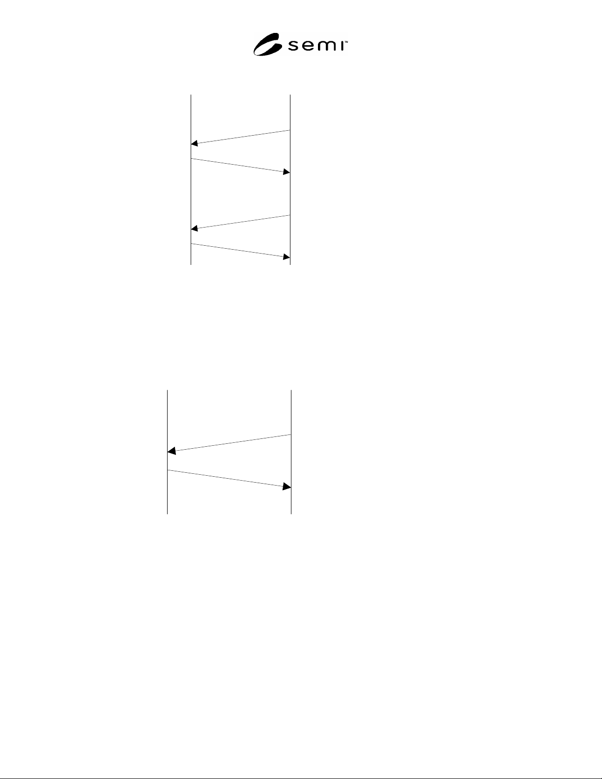
R1-3 Write ID
R1-3.1 The CIDRW is in IDLE. The upstream controller requests the CIDRW change its operational status to
MAINTENANCE.
R1-3.2 The CIDRW changes to MAINTENANCE and replies that it has changed state.
R1-3.3 The upstream controller sends a Write ID Request message to the CIDRW for Head 1. The CIDRW Head 1
reads the ID, and the CIDRW returns the ID to the upstream controller.
SEMI E99.1-1104 © SEMI 2000, 2004 6
CIDRW
Upstream
Controller
S18,F13 Subsystem
Command Request
Target ID = “00”
CPVAL = “OP”, “MT”
S18,F14 Subsystem
Command Acknowledge
SSACK = “NO”
S18,F11 Write ID
Target ID = “01”
MID = “ABC”
S18,F12 Write ID Data
SSACK = “NO”
Figure R1-3
Write ID Data Scenario
R1-4 Write Data
R1-4.1 The upstream controller sends a Write Data Request message to the CIDRW for Head 1 and DataSeg 1.
The CIDRW Head 1 writes the data, and the CIDRW returns the results to the upstream controller.
CIDRW
Upstream
Controller
S18,F7 Write Data Request
Target ID = “01”
DataSeg = “0”
Data = “xxxxxxx”
S18,F8 Write Data
Acknowledge
SSACK = “NO”
Figure R1-4
Write Data Scenario
NOTICE: SEMI makes no warranties or representations as to the suitability of the standard set forth herein for any
particular application. The determination of the suitability of the standard is solely the responsibility of the user.
Users are cautioned to refer to manufacturer’s instructions, product labels, product data sheets, and other relevant
literature respecting any materials mentioned herein. These standards are subject to change without notice.
The user’s attention is called to the possibility that compliance with this standard may require use of copyrighted
material or of an invention covered by patent rights. By publication of this standard, SEMI takes no position
respecting the validity of any patent rights or copyrights asserted in connection with any item mentioned in this
standard. Users of this standard are expressly advised that determination of any such patent rights or copyrights, and
the risk of infringement of such rights, are entirely their own responsibility.
Copyright by SEMI® (Semiconductor Equipment and Materials
International), 3081 Zanker Road, San Jose, CA 95134. Reproduction of
the contents in whole or in part is forbidden without express written
consent of SEMI.